Google is testing AI to respond to privacy requests
Robotic customer support fails while pretending to be an outsourced human. Last week I searched with Google for Elphel and I got a wrong spelled name, wrong address and a wrong phone number.
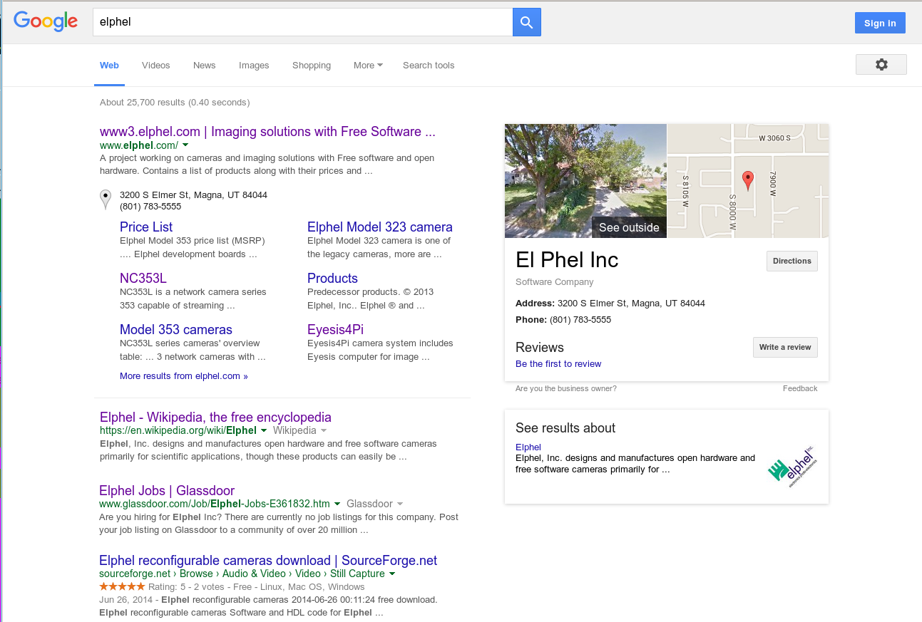
Google search for Elphel
A week ago I tried Google Search for our company (usually I only check recent results using last week or last 3 days search) and noticed that on the first result page there is a Street View of my private residence, my home address pointing to a business with the name “El Phel, Inc”.
Yes, when we first registered Elphel in 2001 we used our home address, and even the first $30K check from Google for development of the Google Books camera came to this address, but it was never “El Phel, Inc.” Later wire transfers with payments to us for Google Books cameras as well as Street View ones were coming to a different address – 1405 W. 2200 S., Suite 205, West Valley City, Utah 84119. In 2012 we moved to the new building at 1455 W. 2200 S. as the old place was not big enough for the panoramic camera calibration.
I was not happy to see my house showing as the top result when searching for Elphel, it is both breach of my family privacy and it is making harm to Elphel business. Personally I would not consider a 14-year old company with international customer base a serious one if it is just a one-man home-based business. Sure you can get the similar Street View results for Google itself but it would not come out when you search for “Google”. Neither it would return wrongly spelled business name like “Goo & Gel, Inc.” and a phone number that belongs to a Baptist church in Lehi, Utah (update: they changed the phone number to the one of Elphel).
Google original location
Honestly there was some of our fault too, I’ve seen “El Phel” in a local Yellow Pages, but as we do not have a local business I did not pay attention to that – Google was always good at providing relevant information in the search results, extracting actual contact information from the company “Contacts” page directly.
Noticing that Google had lost its edge in providing search results (Bing and Yahoo show relevant data), I first contacted Yellow Pages and asked them to correct information as there is no “El Phel, Inc.” at my home address and that I’m not selling any X-Ray equipment there. They did it very promptly and the probable source of the Google misinformation (“probable” as Google does not provide any links to the source) was gone for good.
I waited for 24 hours hoping that Google will correct the information automatically (post on Elphel blog appears in Google search results in 10 – 19 seconds after I press “Publish” button). Nothing happened – same “El Phel, Inc.” in our house.
So I tried to contact Google. As Google did not provide source of the search result, I tried to follow recommendations to correct information on the map. And the first step was to log in with Google account, since I could not find a way how to contact Google without such account. Yes, I do have one – I used Gmail when Google was our customer, and when I later switched to other provider (I prefer to use only one service per company, and I selected to use Google Search) I did not delete the Gmail account. I found my password and was able to log in.
First I tried to select “Place doesn’t exist” (There is no such company as “El Phel, Inc.” with invalid phone number, and there is no business at my home address).
Auto confirmation came immediately:
From: Google Maps <noreply-maps-issues@google.com>
Date: Wed, Sep 23, 2015 at 9:55 AM
Subject: Thanks for the edit to El Phel Inc
To: еlphеl@gmаil.cоm
Maps
Thank you
Your edit is being reviewed. Thanks for sharing your knowledge of El Phel Inc.
El Phel Inc
3200 Elmer St, Magna, UT, United States
Your edit
Place doesn't exist
Edited on Sep 23, 2015 · In review
Keep exploring,
The Google Maps team
© 2015 Google Inc. 1600 Amphitheatre Parkway, Mountain View, CA 94043
You've received this confirmation email to update you about your editing activities on Google Maps.
But nothing happened. Two days later I tried with different option (there was no place to provide text entry)
Your edit
Place is private
No results either.
Then I tried to follow the other link after the inappropriate search result – “Are you the business owner?” (I’m not at owner of the non-existing business, but I am an owner of my house). And yes, I had to use my Gmail account again. There were several options how I prefer to be contacted – I selected “by phone”, and shortly after a female-voiced robot called. I do not have a habit of talking to robots, so I did not listen what it said waiting for keywords like: “press 0 to talk to a representative” or “Please stay on the line…”, but it never said anything like this and immediately hang up.
Second time I selected email contact, but it seems to me that the email conversation was with some kind of Google Eliza. This was the first email:
From : local-help@google.com
To : andrey@elphel.com
Subject : RE: [7-2344000008781] Google Local Help
Date : Thu, 24 Sep 2015 22:48:47 -0700
Add Label
Hi,
Greetings from Google.
After investigating, i found that here is an existing page on Google (El Phel Inc-3200 S Elmer St Magna, UT 84044) which according to your email is incorrect information.
Apologies for the inconvenience andrey, however as i can see that you have created a page for El Phel Inc, hence i would first request you to delete the Business page if you aren't running any Business. Also you can report a problem for incorrect information on Maps,Here is an article that would provide you further clarity on how to report a problem or fix the map.
In case you have any questions feel free to reply back on the same email address and i would get back to you.
Regards,
Rohit
Google My Business Support.
This robot tried to mimic a kids language (without capitalizing “I” and the first letter of my name), and the level of understanding the matter was below that of a human (it was Google, not me who created that page, I just wanted it to be removed).
I replied as I thought it still might be a human, just tired and overwhelmed by so many privacy-related requests they receive (the email came well after hours in United States).
From : andrey <andrey@elphel.com>
To : local-help@google.com
Subject : RE: [7-2344000008781] Google Local Help
Date : Fri, 25 Sep 2015 00:16:21 -0700
Hello Rohit,
I never created such page. I just tried different ways to contact Google to remove this embarrassing link. I did click on "Are you the business owner" (I am the owner of this residence at 3200 S Elmer St Magna, UT 84044) as I hoped that when I'll get the confirmation postcard I'll be able to reply that there is no business at this residential address).
I did try link "how to report a problem or fix the map", but I could not find a relevant method to remove a search result that does not reference external page as a source, and assigns my home residence to the search results of the company, that has a different (than listed) name, is located in a different city (West Valley City, 84119, not in Magna, 84044), and has a different phone number.
So please, can you remove that incorrect information?
Andrey Filippov
Nothing happened either, then on Sunday night (local time) came another email from “Rohit”:
From : local-help@google.com
To : andrey@elphel.com
Subject : RE: [7-2344000008781] Google Local Help
Date : Sun, 27 Sep 2015 18:11:44 -0700
Hi,
Greetings from Google.
I am working on your Business pages and would let you know once get any update.
Please reply back on the same email address in case of any concerns.
Regards,
Rohit
Google My Business Support
You may notice that it had the same ticket number, so the sender had all the previous information when replying. For any human capable of using just Google Search it would be not more than 15-30 seconds to find out that their information is incorrect and either remove it completely (as I asked) or replace with some relevant one.
And there is another detail that troubles me. Looking at the time/days when the “Google My Business Support” emails came, and the name “Rohit” it may look like it came from India. While testing a non-human communications Google might hope that correspondents would more likely attribute some inconsistencies in the generated emails to the cultural differences and miss actual software flaws. Does Google count on us being somewhat racists?
Following provided links I was not able to get any response from a human representative, only two robots (phone and email) contacted me. I hope that this post will work better and help to cure this breach of my family privacy and end harm this invalid information provided by a so respected Internet search company causes to the business. I realize that robots will take over more and more of our activities (and we are helping that to happen ourselves), but maybe this process sometimes goes too fast?
10393
← Older revision
Revision as of 02:16, 26 September 2015
(9 intermediate revisions not shown)Line 1:
Line 1:
-More info to be added, starting with [[Media:10393.pdf|10393 Circuit Diagram, Parts List, PCB layout]]+[[Image:10393_top_sm.png|frame|[[Media:10393_top.jpeg|10393 board, top view]]]]
+[[Image:10393_bottom_sm.png|frame|[[Media:10393_bottom.jpeg|10393 board, bottom view]]]]
+[[Image:10393_bd.png|frame|[[Media:10393.pdf|10393 Circuit Diagram, Parts List, PCB layout]] [[Media:10393_gerber.tar.gz|10353 Gerber files]]]]
+10393 is the system board of Elphel NC393 series camera. It will also replace [[10353|10353 board]] in [[Elphel_Eyesis4Pi|Eyesis4pi]] and other Elphel multi-sensor cameras. It has the same physical dimensions as 10353 and may be used as an upgrade to the previous camera modules.
+
+This camera system board is designed to simultaneously support multiple sensors - both with legacy parallel interface (it is directly compatible with [[10338|10338 Sensor board]] and [[10359|10359 Sensor multiplexer board]]) and with new high-speed serial interface (up to 8 lanes + clock per each port). Sensor ports of the 10393 can be combined to interface larger/higher speed sensors, interface supply voltage is programmable in the range of 1.35V to 2.8V. All the sensor port interface signals are routed directly to the FPGA pads (22 I/O signals on each of the 4 flex cable connectors) , so the same ports can be uses for other purposes, for example to control the motors or interface IMU of the quadcopter.
+
+Block diagram below shows major parts and I/O ports of the 10393 board. Left edge of the diagram corresponds to the sensor connections, right one - to the camera back panel with external connectors, top and bottom contain inter-board connections:
+* The system is built around Xilinx Zynq 7030 SoC that combines a dual-core ARM processor, a rich set of the standard peripherals and FPGA on the same chip. This combination provides high bandwidth connection between the processors and the FPGA fabric.
+* 4 identical sensor ports are 30-conductor 0.5mm pitch flex cable connectors, compatible with the earlier Elphel products. These connectors are split into two pairs, so they are closest to one short edge of the board - two on each side. Combined with an external multiplexer boards (at the expense of proportionally lower frame rate) each 10393 can work with up to 16 sensors (12 with the existing [[10359|10359 board]]).
+* 500MB of the dedicated DDR3 memory chip is connected directly to the FPGA portion of the SoC, with the 16-channel image-optimized controller it provides efficient access to the memory for simultaneous image acquisition, compression and image processing. We plan to implement such functionality as real-time image de-warping and correlation of images from multiple sensors for the 3d data extraction.
+* 1GB of DDR3 memory (2 chips providing 32-bit data bus) is uses as a system RAM for the processor subsystem.
+* 500MB of NAND flash provide program storage.
+* Persistent program storage is expandable with the micro-SD cards (not easy to see on the photo as the slot is hidden under the network connector). This interface provides bootable memory, so it is always possible to restore the camera functionality even if the system NAND will be accidentally flashed with corrupted image.
+* Largest visible component on the board is the RJ45 connector for the Gigabit Ethernet, containing all the required magnetics (transformers) that are compatible with the PoE application. The peculiar shape of the board near connector is designed that it can be used with the hardware of the sealed RJ45 connectors.
+* On the other side of the PCB under the RJ45 connector is the micro-USB connector type B (device) that can be used to implement a system console for camera software development. Additionally the USB-to-serial converter in on the 10393 board has GPIO functionality, it makes it possible to remotely reset/reboot the camera as well to as select the boot source (on the board NAND flash or external memory card). It also allows to build a fail-safe autonomous system with a camera reset-over-USB generated by a different master.
+* 10353 uses 3.3VDC as a primary power source. All other voltages required by the SoC and other subsystems are generated from this primary 3.3 by the "Secondary power module" that includes fixed and adjustable by the software (over i2c bus) voltages, some voltages (such as sensor power) can be programmatically turned on or off. Primary 3.3VDC are provided by a separate [[10385|10385 power supply board]] that can be shut down by the software and awaken by an alarm signal from the clock/calendar.
+* Clock/calendar uses a super-capacitor (large black cylinder on the bottom view photo) to provide power when the camera is turned off. This allows camera to be used to record time-lapse images during extended periods with only a battery, possibly combined with a small solar panel.
+* Extension port uses a high-density 40-pin connector to interface a [[10389|10389 Extension board]]. It provides USB (host) signals, SATA channel, system i2c and GPIO signals from the FPGA. Extension board provides:
+** SSD mass storage in m.2 SATA form-factor (up to 2260 - 22mm x 60mm).
+** USB host (micro-A) external connector.
+** eSATA/USB combo connector that can be used to connect USB flash drives, external HDD/SDD (powered externally or by USB 5.0V power) and host computer for high-speed data transfer (SATA3.0 - 6GHz)form the internal SSD storage.
+** Inter-camera external synchronization connector (2.5mm audio type).
+** Inter-camera module synchronization with a 4-conductor flex cables.
+** Two of the 10-conductor flex cable ports that carry 3.3VDC, 5.0VDC, USB, i2c and GPIO, compatible with existing [[103695|103695 IMU adapter]] and [[103696|103696 GPS adapter]] boards.
Andrey.filippov
10393
← Older revision
Revision as of 01:41, 26 September 2015
(3 intermediate revisions not shown)Line 1:
Line 1:
-More info to be added, starting with [[Media:10393.pdf|10393 Circuit Diagram, Parts List, PCB layout]]+[[Image:10393_top_sm.png|frame|[[Media:10393_top.jpeg|10393 board, top view]]]]
+[[Image:10393_bottom_sm.png|frame|[[Media:10393_bottom.jpeg|10393 board, bottom view]]]]
+[[Image:10393_bd.png|frame|[[Media:10393.pdf|10393 Circuit Diagram, Parts List, PCB layout]] [[Media:10393_gerber.tar.gz|10353 Gerber files]]]]
+10393 is the system board of Elphel NC393 series camera. It will also replace [[10353|10353 board]] in [[Elphel_Eyesis4Pi|Eyesis4pi] and other Elphel multi-sensor cameras. It has the same physical dimensions as 10353 and may be used as an upgrade to the previous camera modules.
+
+This camera system board is designed to simultaneously support multiple sensors - both with legacy parallel interface (it is directly compatible with [[10338|10338 Sensor board]] and [[10359|10359 Sensor multiplexer board]]) and with new high-speed serial interface (up to 8 lanes + clock per each port). Sensor ports of the 10393 can be combined to interface larger/higher speed sensors, interface supply voltage is programmable in the range of 1.35V to 2.8V. All the sensor port interface signals are routed directly to the FPGA pads (22 I/O signals on each of the 4 flex cable connectors) , so the same ports can be uses for other purposes, for example to control the motors or interface IMU of the quadcopter.
+
+Block diagram below shows major parts and I/O ports of the 10393 board. Left edge of the diagram corresponds to the sensor connections, right one - to the camera back panel with external connectors, top and bottom contain inter-board connections:
+* The system is built around Xilinx Zync SoC that combines a dual-core ARM processor, a rich set of the standard peripherals and FPGA on the same chip. This combination provides high bandwidth connection between the processors and the FPGA fabric.
+* 4 identical sensor ports are 30-conductor 0.5mm pitch flex cable connectors, compatible with the earlier Elphel products. These connectors are split into two pairs, so they are closest to one short edge of the board - two on each side. Combined with an external multiplexer boards (at the expense of proportionally lower frame rate) each 10393 can work with up to 16 sensors (12 with the existing [[10359|10359 board]]).
+* 500MB of the dedicated DDR3 memory chip is connected directly to the FPGA portion of the SoC, with the 16-channel image-optimized controller it provides efficient access to the memory for simultaneous image acquisition, compression and image processing. We plan to implement such functionality as real-time image de-warping and correlation of images from multiple sensors for the 3d data extraction.
+* 1GB of DDR3 memory (2 chips providing 32-bit data bus) is uses as a system RAM for the Processor subsystem.
+* 500MB of NAND flash provide program storage.
+* Persistent program storage is expandable with the micro-SD cards (not easy to see on the photo as the slot is hidden under the network connector). This interface provides bootable memory, so it is always possible to restore the camera functionality even if the system NAND will be accidentally flashed with corrupted image.
+* Largest visible component on the board is the RJ45 connector for the Gigabit Ethernet, containing all the required magnetics (transformers) that are compatible with the PoE application. The peculiar shape of the board near connector is designed that it can be used with the hardware of the sealed RJ45 connectors.
+* On the other side of the PCB under the RJ45 connector is the micro-USB connector type B (device) that can be used to implement a system console for camera software development. Additionally the USB-to-serial converter in on the 10393 board has GPIO functionality, it makes it possible to remotely reset/reboot the camera as well to as select the boot source (on the board NAND flash or external memory card). It also allows to build a fail-safe autonomous system with a camera reset-over-USB generated by a different master.
Andrey.filippov
10393
← Older revision
Revision as of 00:14, 26 September 2015
Line 1:
Line 1:
-More info to be added, starting with [[Media:10393.pdf|10393 Circuit Diagram, Parts List, PCB layout]]+[[Image:10393_top_sm.png|frame|[[Media:10393_top.jpeg|10393 board, top view]]]]
+[[Image:10393_bottom_sm.png|frame|[[Media:10393_bottom.jpeg|10393 board, bottom view]]]]
+[[Image:10393_bd.png|frame|[[Media:10393.pdf|10393 Circuit Diagram, Parts List, PCB layout]] [[Media:10393_gerber.tar.gz|10353 Gerber files]]]]
Andrey.filippov
File:10393 gerber.tar.gz
uploaded "[[File:10393 gerber.tar.gz]]"
Andrey.filippovFile:10393 bottom sm.png
uploaded "[[File:10393 bottom sm.png]]"
Andrey.filippov
Yocto tests
Setup:
← Older revision Revision as of 02:40, 25 September 2015 (4 intermediate revisions not shown)Line 25: Line 25: * '''uramdisk.image.gz''' - applications * '''uramdisk.image.gz''' - applications Copy them on the micro SD card > run '''boot''' once in the u-boot command line. Copy them on the micro SD card > run '''boot''' once in the u-boot command line. + + +==<font color="blue">Boot options</font>== +a. Unpack the root file system image to RAM at boot time. + +Check u-boot config file. + +Keep '''uramdisk.image.gz''' along with other files on FAT partition. + +b. Keep the root file system on EXT2(EXT3,etc.) partition of SD card. + +Create '''uEnv.txt''' on FAT partition. ''uEnv.txt'': + uenv_boot=fatload mmc 0 0x3F00000 ${kernel_image} && fatload mmc 0 0x3E00000 ${devicetree_image} && bootm 0x3F00000 - 0x3E00000 + uenvcmd=run uenv_boot + +Devicetree needs to be recompiled with changes in ''bootargs''-line: + +for ext2: + root=/dev/mmcblk0p2 +for ram: + root=/dev/ram ==<font color="blue">Setup</font>== ==<font color="blue">Setup</font>== Line 34: Line 55: cd poky; git checkout 50e9ccb2aff7b9f9dca4fda99a6832c60f64de3b cd poky; git checkout 50e9ccb2aff7b9f9dca4fda99a6832c60f64de3b - git clone -b dora https://github.com/openembedded/meta-oe.git meta-oe+ git clone -b dora https://github.com/openembedded/meta-oe.git meta-oe + #'''has changed to git clone -b fido https://github.com/openembedded/meta-openembedded?!!!!!!!!''') cd meta-oe; git checkout ee173678383683e972c7d4d6f0ef5790bfa50274; cd .. cd meta-oe; git checkout ee173678383683e972c7d4d6f0ef5790bfa50274; cd .. Line 138: Line 160: ====Notes==== ====Notes==== <font size='2'> <font size='2'> +* Select root file system format in the recipe: + IMAGE_FSTYPES = "tar.gz" * Current packages: * Current packages: - ''elphel393.bb'':+ ''core-image-elphel393.bb'': IMAGE_INSTALL = "packagegroup-core-boot python-core ${ROOTFS_PKGMANAGE_BOOTSTRAP} ${CORE_IMAGE_EXTRA_INSTALL}" IMAGE_INSTALL = "packagegroup-core-boot python-core ${ROOTFS_PKGMANAGE_BOOTSTRAP} ${CORE_IMAGE_EXTRA_INSTALL}" * Also works: * Also works: - ''elphel393.bb'':+ ''core-image-elphel393.bb'': IMAGE_INSTALL = "packagegroup-core-boot ${ROOTFS_PKGMANAGE_BOOTSTRAP} ${CORE_IMAGE_EXTRA_INSTALL}" IMAGE_INSTALL = "packagegroup-core-boot ${ROOTFS_PKGMANAGE_BOOTSTRAP} ${CORE_IMAGE_EXTRA_INSTALL}" IMAGE_INSTALL_append = "python-core" IMAGE_INSTALL_append = "python-core" Line 334: Line 358: Regards, Regards, Nathan Nathan + +==<font color="blue">Some links</font>== +* http://picozed.org/content/microzed-how-boot-sd-card +* http://zedboard.org/content/cannot-use-sd-card-partition-root-filesystem +* http://architechboards-microzed.readthedocs.org/en/latest/quick.html +* http://architechboards-microzed.readthedocs.org/en/latest/board.html + +1. u-boot environment variables: +print all: + ~: printenv + +setenv examples: + ~: setenv modeboot "run uenvboot" + ~: setenv uenvboot "fatload mmc 0 0x3000000 uEnv.txt && env import -t 0x3000000 $filesize && run uenv_boot" + +2. Unpack image into SD card ext2 partition: + +sudo tar -xzf core-image-minimal-dev-microzed.tar.gz -C /media/rootfs/ OlegNC393 progress update: all hardware is operational
10393 with 4 image sensors
Finally all the parts of the NC393 prototype are tested and we now can make the circuit diagram, parts list and PCB layout of this board public. About the half of the board components were tested immediately when the prototype was built – it was almost two years ago – those tests did not require any FPGA code, just the initial software that was mostly already available from the distributions for the other boards based on the same Xilinx Zynq SoC. The only missing parts were the GPL-licensed initial bootloader and a few device drivers.
Implementation of the 16-channel DDR3 memory controller
Getting to the next part – testing of the FPGA-controlled DDR3 memory took us longer: the overall concept and the physical layer were implemented in June 2014, timing calibration software and application modules for image image recording and retrieval were implemented in the spring of 2015.
Initial image acquisition and compressionWhen the memory was proved operational what remained untested on the board were the sensor connections and the high speed serial links for SATA. I decided not to make any temporary modules just to check the sensor physical connections but to port the complete functionality of the image acquisition, processing and compression of the existing NC353 camera (just at a higher clock rate and multiple channels instead of a single one) and then test the physical operation together with all the code.
Sensor acquisition channels: From the sensor interface to the video memory bufferThe image acquisition code was ported (or re-written) in June, 2015. This code includes:
- Sensor physical interface – currently for the existing 10338 12-bit parallel sensor front ends, with provisions for the up to 8-lanes + clock high speed serial sensors to be added. It is also planned to bond together multiple sensor channels to interface single large/high speed sensor
- Data and clock synchronization, flexible phase adjustment to recover image data and frame format for different camera configurations, including sensor multiplexers such as the 10359 board
- Correction of the lens vignetting and fine-step scaling of the pixel values, individual for each of the multiplexed sensors and color channel
- Programmable gamma-conversion of the image data
- Writing image data to the DDR3 image buffer memory using one or several frame buffers per channel, both 8bpp and 16bpp (raw image data, bypassing gamma-conversion) formats are supported
- Calculation of the histograms, individual for each color component and multiplexed sensor
- Histograms multiplexer and AXI interface to automatically transfer histogram data to the system memory
- I²c sequencer controls image sensors over i²c interface by applying software-provided register changes when the designated frame starts, commands can be scheduled up to 14 frames in advance
- Command frame sequencer (one per each sensor channel) schedules and applies system register writes (such as to control compressors) synchronously to the sensors frames, commands can be scheduled up to 14 frames in advance
Image compressors get the input data from the external video buffer memory organized as 16×16 pixel macroblocks, in the case of color JPEG images larger overlapping tiles of 18×18 (or 20×20) pixels are needed to interpolate “missing” colors from the input Bayer mosaic input. As all the data goes through the buffer there is no strict requirement to have the same number of compressor and image acquisition modules, but the initial implementation uses 1:1 ratio and there are 4 identical compressor modules instantiated in the design. The compressor output data is multiplexed between the channels and then transferred to the system memory using 1 or 2 of Xilinx Zynq AXI HP interfaces.
This portion of the code is also based on the earlier design used in the existing NC353 camera (some modules are reusing code from as early as 2002), the new part of the code was dealing with a flexible memory access, older cameras firmware used hard-wired 20×20 pixel tiles format. Current code contains four identical compressor channels providing JPEG/JP4 compression of the data stored in the dedicated DDR3 video buffer memory and then transferring result to the system memory circular buffers over one or two of the Xilinx Zynq four AXI HP channels. Other camera applications that use sensor data for realtime processing rather than transferring all the image data to the host may reduce number of the compressors. It is also possible to use multiple compressors to work on a single high resolution/high frame rate sensor data stream.
Single compressor channel contains:
- Macroblock buffer interface requests 32×18 or 32×16 pixel tiles from the memory and provides 18×18 overlapping macroblocks for JPEG or 16×16 non-overlapping macroblocks for JP4 using 4KB memory buffer. This buffer eliminates the need to re-read horizontally overlapping pixels when processing consecutive macroblocks
- Pixel buffer interface retrieves data from the memory buffer providing sequential pixel stream of 18×18 (16×16) each macroblock
- Color conversion module selects one of the sub-modules : csconvert18a, csconvert_mono, csconvert_jp4 or csconvertjp4_diff to convert possibly overlapping Bayer mosaic tiles to a sequence of 8×8 blocks for 2-d DCT transform
- Average value extractor calculates average value in each 8×8 block, subtracts it before DCT and restores after – that reduces data width in DCT processing module
- xdct393 performs 2-d DCT for each 8×8 pixel block
- Quantizer re-orders each block DCT components from the scan-line to zigzag sequence and quantizes them using software-calculated and loaded tables. This is the only lossy stage of the JPEG algorithm, when the compression quality is set to 100% all the coefficients are set to 1 and the conversion is lossless
- Focus sharpness module accumulates amount of high-frequency components to estimate image sharpness over specified window to facilitate (auto) focusing. It also allows to replace on-the-fly average block value of the image with amount of the high frequency components in the same blog, providing visual indication of the focus sharpness
- RLL encoder converts the continuous 64 samples/per block data stream in to RLL-encoded data bursts
- Huffman encoder uses software-generated tables to provide additional lossless compression of the RLL-encoded data. This module (together with the next one) runs and double pixel clock rate and has an input FIFO between the clock domains
- Bit stuffer consolidates variable length codes coming out from the Huffman encoder into fixed-width words, escaping each 0xff byte (these bytes have special meaning in JPEG stream) by inserting 0×00 right after it. It additionally provides image timestamp and length in bytes after the end of the compressed data before padding the data to multiple of 32-byte chunks, this metadata has fixed offset before the 32-byte aligned data end
- Compressor output FIFO converts 16-bit wide data from the bit stuffer module received at a double compressor clock rate (currently 200MHz) and provides 64-bit wide output at the maximal clock rate (150MHz) for AXI HP port of Xilinx Zynq, it also provides buffering when several compressor channels share the same AXI HP channel
Another module – 4:1 compressor multiplexer is shared between multiple compressor channels. It is possible (defined by Verilog parameters) to use either single multiplexer with one AXI HP port (SAXIHP1) and 4 compressor inputs (4:1), or two of these modules interfacing two AXI HP channels (SAXIHP1 and SAXIHP2), reducing number of concurrent inputs of each multiplexer to just 2 (2 × 2:1). Multiplexers use fair arbitration policy and consolidate AXI bursts to full 16×64bits when possible. Status registers provide image data pointers for last write and last frame start, each as sent to AXI and after confirmation using AXI write response channel.
Porting remaining FPGA functionality to the new cameraAdditional modules where ported to complete the existing NC353 functionality:
- Camera real time clock that provides current time with 1 microsecond resolution to various modules. It has accumulator-based correction circuitry to compensate for crystal oscillator frequency variations
- Inter-camera synchronization module generates and/or receives synchronization signals between multiple camera modules or other devices. When used between the cameras, each synchronization pulse has a timestamp information attached in a serialized form, so multiple synchronized cameras have all the simultaneous images metadata contain the same time code generated by the “master” camera
- Event logger records data from multiple sources, such as GPS, IMU, image acquisition events and external signal channel (like a vehicle wheel rotation sensor)
All that code was written (either new or modified from the existing NC353 FPGA project by the end of July, 2015 and then the most fun began. First I used the proven NC353 code to simulate (using Icarus Verilog + GtkWave) with the same input data as the one provided to the new x393 code, following the signal chains and making sure that each checkpoint data matched. That was especially useful when debugging JPEG compressor, as the intermediate data is difficult to follow. When I was developing the first JPEG compressor in 2002 I had to save output data from the various processing stages and compare it to the software compression output of the same image data from the similar stages. Having working implementation helped a lot and in 3 weeks I was able to match the output from all the processing stages described above except the event logger that I did not verify yet.
Testing the hardwareThen it was the time for translating the Verilog test fixture code to the Python programs running on the target hardware extending the code developed earlier for the memory controller. The code is able to parse Verilog parameter definition files – that simplified synchronization of the Verilog and Python code. It would be nice to use something like Cocotb in the future and completely get rid of the Verilog to Python manual translation.
As I am designing code for the reconfigurable FPGA (not for ASIC) my usual strategy is not to get high simulation coverage, but to simulate to a “barely working” stage, then use the actual hardware (that runs tens of millions times faster than the simulator), detect the problems and then try to achieve the same condition with the simulation. But when I just started to run the hardware I realized that there is too little I can get about the current state of the hardware. Remembering about the mess of the temporary debug code I had in the previous projects and the inability of the synthesis tool to directly access the qualified names of the signals inside sub-modules, I implemented rather simple debug infrastructure that uses a single register ring (like a simplified JTAG) through all the modules to debug and a matching Python code that allows access to individual bit fields of the ring. Design includes a single debug_master and debug_slave modules in each of the design module instances that needs debugging (and the modules above – up to the top one). By the time the camera was able to generate correct images the total debug ring consisted of almost a hundred of the 32-bit registers, when I later disabled this debug functionality by commenting out a single `define DEBUB_RING macro it recovered almost 5% of the device slices. The program output looks like:
x393 +0.001s--> print_debug 0x38 0x3e
038.00: compressors393_i.jp_channel0_i.debug_fifo_in [32] = 0x6e280 (451200)
039.00: compressors393_i.jp_channel0_i.debug_fifo_out [28] = 0x1b8a0 (112800)
039.1c: compressors393_i.jp_channel0_i.dbg_block_mem_ra [ 3] = 0x3 (3)
039.1f: compressors393_i.jp_channel0_i.dbg_comp_lastinmbo [ 1] = 0x1 (1)
03a.00: compressors393_i.jp_channel0_i.pages_requested [16] = 0x26c2 (9922)
03a.10: compressors393_i.jp_channel0_i.pages_got [16] = 0x26c2 (9922)
03b.00: compressors393_i.jp_channel0_i.pre_start_cntr [16] = 0x4c92 (19602)
03b.10: compressors393_i.jp_channel0_i.pre_end_cntr [16] = 0x4c92 (19602)
03c.00: compressors393_i.jp_channel0_i.page_requests [16] = 0x4c92 (19602)
03c.10: compressors393_i.jp_channel0_i.pages_needed [16] = 0x26c2 (9922)
03d.00: compressors393_i.jp_channel0_i.dbg_stb_cntr [16] = 0xcb6c (52076)
03d.10: compressors393_i.jp_channel0_i.dbg_zds_cntr [16] = 0xcb6c (52076)
03e.00: compressors393_i.jp_channel0_i.dbg_block_mem_wa [ 3] = 0x4 (4)
03e.03: compressors393_i.jp_channel0_i.dbg_block_mem_wa_save [ 3] = 0x0 (0)
All the problems I encountered while trying to make hardware work turned out to be reproducible (but no always easy) with the simulation and the next 3 weeks I was eliminating then one by one. When I’ve got to the 51-st version of the FPGA bitstream file (there were several more when I forgot to increment version number) camera started to produce consistently valid JPEG files.
First 4-sensor image acquired with NC393 camera
At that point I replaced a single sensor front end with no lens attached (just half of the input sensor window was covered with a tape to produce a blurry shadow in the images) with four complete SFE with lenses simultaneously using a piece of Eyesis4π hardware to point the individual sensors at the 45° angles (in portrait mode) covering 180°×60° FOV combined – it resulted in the images shown above. Sensor color gains are not calibrated (so there is visible color mismatch) and the images are not stitched together (just placed side-by-side) but i consider it to be a significant milestone in the NC393 camera development.
SATA controller statusAlmost at the same time Alexey who is working on SATA controller for the camera achieved an important milestone too. His code running in Xilinx Zynq was able to negotiate and establish link with an mSATA SSD connected to the NC393 prototype. There is still a fair amount of design work ahead until we’ll be able to use this controller with the camera, but at least the hardware operation of this part of the design is verified now too.
What is nextHaving all the hardware on the 10393 verified we are now able to implement minor improvements and corrections to the 3 existing boards of the NC393 camera:
- 10393 itself
- 10389 – extension board with mSATA SSD, eSATA/USB combo connector, micro-USB and synchronization I/O
- 10385 – power supply board
And then make the first batch of the new cameras that will be available for other developers and customers.
We also plane to make a new sensor board with On Semiconductor (former Aptina, former Micron) MT9F002 – 14MPix sensor with the same 1/2.3″ image format as the MT9F006 used with the current NC353 cameras. This 12-bit sensor will allow us to try multi-lane high speed serial interface keeping the same physical dimension of the sensor board and use the same lenses as we use now.
Ezynq
Changed link to current repository at GitHub
← Older revision Revision as of 05:35, 17 September 2015 Line 1: Line 1: ==Decription== ==Decription== -[https://sourceforge.net/p/elphel/ezynq Ezynq] project is started to create a bootloader for systems based on the Xilinx Zynq SoC without the inconvenience of the non-free tools and/or files. The goal is not just to "free" the code, but to provide users with the higher degree of flexibility in fine-tuning of the configuration parameters.+[https://github.com/Elphel/ezynq Ezynq] project is started to create a bootloader for systems based on the Xilinx Zynq SoC without the inconvenience of the non-free tools and/or files. The goal is not just to "free" the code, but to provide users with the higher degree of flexibility in fine-tuning of the configuration parameters. ====="Free" the code part===== ====="Free" the code part===== Line 6: Line 6: * FSBL is under Xilinx's copyright * FSBL is under Xilinx's copyright * The current (2014/02/23) official SPL implementation in the [https://github.com/Xilinx/u-boot-xlnx/tree/master-next u-boot-xlnx master-next 54fee227ef141214141a226efd17ae0516deaf32] branch is FSBL-less but it requires to use the files (<b>ps7_init.c/h</b>) that come under Xilinx's copyright which makes u-boot noncompliant with its GPL license. * The current (2014/02/23) official SPL implementation in the [https://github.com/Xilinx/u-boot-xlnx/tree/master-next u-boot-xlnx master-next 54fee227ef141214141a226efd17ae0516deaf32] branch is FSBL-less but it requires to use the files (<b>ps7_init.c/h</b>) that come under Xilinx's copyright which makes u-boot noncompliant with its GPL license. - ==Supported boards== ==Supported boards== Andrey.filippov10393
Created page with "More info to be added, starting with 10393 Circuit Diagram, Parts List, PCB layout"
New page
More info to be added, starting with [[Media:10393.pdf|10393 Circuit Diagram, Parts List, PCB layout]] Andrey.filippovFile:10393.pdf
uploaded "[[File:10393.pdf]]" Circuit diagram and PCB layout for the 10393 Rev 0 board
Andrey.filippovElphel 353 series quick start guide
← Older revision
Revision as of 22:02, 16 September 2015
(6 intermediate revisions not shown)Line 88:
Line 88:
|[[image:Display live video.jpeg|250px|thumb|Fig. 7 Turn on Live Video Stream]] |[[image:Display live video.jpeg|250px|thumb|Fig. 7 Turn on Live Video Stream]]
|} |}
-====2. watch: player GUI / command line====+
-To watch the video stream with MPlayer or VLC open the '''rtsp://192.168.0.9:554'''. You can use either a player GUI or a command line. Here is an example command from Linux terminal window: +====2. watch: multipart jpeg (low latency)====
+* Works in Firefox, '''low latency stream'''
+ '''http://192.168.0.9:8081/mimg'''
+
+====3. watch: player GUI / command line====
+To watch the video stream with VLC or something else (ffplay, Mplayer) open the '''rtsp://192.168.0.9:554'''. You can use either a player GUI or a command line. Here is an example command from Linux terminal window:
+<!--
+Doesn't work anymore?!
=====Mplayer===== =====Mplayer=====
'''mplayer rtsp://192.168.0.9:554 -vo x11 -zoom''' '''mplayer rtsp://192.168.0.9:554 -vo x11 -zoom'''
-=====VLC=====+-->
- '''vlc rtsp://192.168.0.9:554 -V x11 --rtsp-caching=50''' +=====VLC (high latency, ffplay might be better)=====
-The default setting for rtsp-caching is 5000 milliseconds which means the stream is delayed 5 seconds which is not very handy for real-time video preview so the above commands starts VLC with it set to 50 ms+ '''vlc rtsp://192.168.0.9:554'''
-====3. record: command line====+====4. record: command line====
'''mencoder rtsp://192.168.0.9:554 -ovc copy -fps <fps> -o <file_name>.mov''' '''mencoder rtsp://192.168.0.9:554 -ovc copy -fps <fps> -o <file_name>.mov'''
Oleg
Elphel 353 series quick start guide
3. watch: player GUI / command line:
← Older revision Revision as of 21:04, 16 September 2015 (One intermediate revision not shown)Line 88: Line 88: |[[image:Display live video.jpeg|250px|thumb|Fig. 7 Turn on Live Video Stream]] |[[image:Display live video.jpeg|250px|thumb|Fig. 7 Turn on Live Video Stream]] |} |} -====2. watch: player GUI / command line====+ -To watch the video stream with MPlayer or VLC open the '''rtsp://192.168.0.9:554'''. You can use either a player GUI or a command line. Here is an example command from Linux terminal window: +====2. watch: multipart jpeg==== +* Works in Firefox, low latency + '''http://192.168.0.9:8081/mimg''' + +====3. watch: player GUI / command line==== +To watch the video stream with VLC or something else open the '''rtsp://192.168.0.9:554'''. You can use either a player GUI or a command line. Here is an example command from Linux terminal window: +<!-- +Doesn't work anymore?! =====Mplayer===== =====Mplayer===== '''mplayer rtsp://192.168.0.9:554 -vo x11 -zoom''' '''mplayer rtsp://192.168.0.9:554 -vo x11 -zoom''' +--> =====VLC===== =====VLC===== '''vlc rtsp://192.168.0.9:554 -V x11 --rtsp-caching=50''' '''vlc rtsp://192.168.0.9:554 -V x11 --rtsp-caching=50''' The default setting for rtsp-caching is 5000 milliseconds which means the stream is delayed 5 seconds which is not very handy for real-time video preview so the above commands starts VLC with it set to 50 ms The default setting for rtsp-caching is 5000 milliseconds which means the stream is delayed 5 seconds which is not very handy for real-time video preview so the above commands starts VLC with it set to 50 ms -====3. record: command line====+====4. record: command line==== '''mencoder rtsp://192.168.0.9:554 -ovc copy -fps <fps> -o <file_name>.mov''' '''mencoder rtsp://192.168.0.9:554 -ovc copy -fps <fps> -o <file_name>.mov''' OlegPHG Post-Processing
Created page with "==Procedures== * Applying pixel mapping information * Aberration correction * Distortion correction * Vignetting correction * Color correction * Denoising * Sharpening ==Require..."
New page
==Procedures==* Applying pixel mapping information
* Aberration correction
* Distortion correction
* Vignetting correction
* Color correction
* Denoising
* Sharpening
==Requirements==
* Linux OS (Kubuntu preferably).
* [[Elphel_Software_Kit_for_Ubuntu#ImageJ_and_Elphel_plugins_for_imageJ|Elphel ImageJ Plugins]].
* Locate calibration kernels for the current camera.
* Locate ''default-config.corr-xml''.
==Instructions==
* Launch ImageJ from Eclipse:
* Go to '''Plugins''' -> '''ImageJ-Elphel''' -> '''Eyesis Correction'''
{|
|- valign="top"
|[[File:Eyesis_corrections_plugin.jpeg|thumb|800px|Eyesis corrections plugin interface]]
|}
* '''Restore''' button -> browse for ''default_config.corr-xml'' (restores parameters for '''Configure correction''')
* '''Configure correction''' button - make sure that the following paths are set correctly (if not - mark the checkboxes - a dialog for each path will pop up):
<font size='2'>
'''Source files directory''' - directory with the footage images
'''Sensor calibration directory''' - [YOUR-PATH]/calibration/sensors
'''Aberration kernels (sharp) directory''' - [YOUR-PATH]/calibration/aberration_kernels/sharp-007
'''Aberration kernels (smooth) directory''' - [YOUR-PATH]/calibration/aberration_kernels/smooth
'''Equirectangular maps directory(may be empty)''' - [YOUR-PATH]/calibration/equirectangular_maps (it should be created automatically if the w/r rights of [YOUR-PATH]/calibration allow)
'''Source file suffix''' - '''.jp4''' if jp4 files are processed
'''Sensor files prefix''' - the format is '''<prefix>NN.calib-tiff''' - '''<prefix>''' is blank if the files are just ''NN.calib-tiff''. For '''XXX-NN.calib-tiff''' the prefix would be '''XXX-'''
'''Sensor files suffix''' - default is '''.calib-tiff'''
'''Kernel files (sharp)/(smooth) prefix - same rule as for the sensor files
'''Kernel files (sharp)/(smooth) suffix''' - default is '''.kernel-tiff'''
'''Equirectangular maps prefix''' - same rule as for the sensor files
'''Equirectangular maps suffix''' - default is '''.eqr-tiff'''
Also the following check boxes need to be checked:
'''De-mosaic'''
'''Sharpen'''
'''Denoise'''
'''Convert colors'''
'''Warp results to equiretangular'''
'''Use projection to a common plane instead of the equirectangular'''
</font>
* '''Configure warping''' (''Skip if the files already exist'') -> rebuild map files - this will create maps in [YOUR-PATH]/calibration/equirectangular_maps. Will take ~5-10 minutes.
* '''Select source files''' -> select all the footage files to be processed - all files should be named as *_1.jp4 (example: test_1.jp4, something was hard coded, we will fix later)
* '''Process files''' to start the processing. Depending on the PC power it can take ~1 minute per image.
[[Category:User Guide]]
[[Category:ImageJ]] Oleg
Elphel Software Kit for Ubuntu
ImageJ and Elphel plugins for imageJ:
← Older revision Revision as of 18:47, 1 September 2015 (One intermediate revision not shown)Line 280: Line 280: It is a very useful tool to do quantitative analysis of the camera images. It is a very useful tool to do quantitative analysis of the camera images. -===ImageJ installation ===+* Download plugins: + git clone https://github.com/Elphel/imagej-elphel.git +* Download [http://www.eclipse.org/downloads/ Eclipse IDE for Java EE Developers] or any other with Maven integration +* Edit ''eclipse.ini'': + -clean -startup + ... + -XX:MaxPermSize=24576m + -Xms2048m + -Xmx24576m +* From Eclipse: + 1. File -> Import -> Existing Maven Projects -> set imagej-elphel as Root Directory - a project will appear in the project list -> Finish + Importing will take some time + + 2. Create Run Configuration: + a. Run Configurations -> select Java Application -> New Launch Configuration -> Search for Aberration_Calibration class and select it -> Run + b. It will launch ''ImageJ & Aberration_Calibration plugin'' + c. Other plugins are launched from ImageJ window from Plugins + +<!-- +=== ImageJ installation === You may download ImageJ bundled with Java from the [http://rsbweb.nih.gov/ij/download.html download page]: You may download ImageJ bundled with Java from the [http://rsbweb.nih.gov/ij/download.html download page]: + ==== With 32-bit Java ==== ==== With 32-bit Java ==== -cd ~/Download; wget "http://rsbweb.nih.gov/ij/download/linux/ij147-linux32.zip" ; unzip ij147-linux32.zip+ cd ~/Downloads; wget "http://rsbweb.nih.gov/ij/download/linux/ij147-linux32.zip" ; unzip ij147-linux32.zip -==== With 64-bit Java ====+ cd ~/Downloads; wget "http://rsbweb.nih.gov/ij/download/linux/ij149-linux64.zip" ; unzip ij149-linux64.zip -cd ~/Download; wget "http://rsbweb.nih.gov/ij/download/linux/ij147-linux64.zip" ; unzip ij147-linux64.zip+ '''If any of the two direct download links above are broken, please use the [http://rsbweb.nih.gov/ij/download.html] to get the new ImageJ version''' '''If any of the two direct download links above are broken, please use the [http://rsbweb.nih.gov/ij/download.html] to get the new ImageJ version''' Line 301: Line 320: Then clone the repository - directly to the ImageJ plugins directory. Provided you used the same directory for ImageJ as written above: Then clone the repository - directly to the ImageJ plugins directory. Provided you used the same directory for ImageJ as written above: cd ~/Downloads/ImageJ/plugins cd ~/Downloads/ImageJ/plugins -<!-- old url: git clone git://elphel.git.sourceforge.net/gitroot/elphel/ImageJ-Elphel -->+ old url: git clone git://elphel.git.sourceforge.net/gitroot/elphel/ImageJ-Elphel git clone git://git.code.sf.net/p/elphel/ImageJ-Elphel git clone git://git.code.sf.net/p/elphel/ImageJ-Elphel Line 314: Line 333: When you'll update the source files, you 'll need to re-run "Compile and run...". meanwhile just use the item in Plugins->ImageJ-Elphel menu. When you'll update the source files, you 'll need to re-run "Compile and run...". meanwhile just use the item in Plugins->ImageJ-Elphel menu. +--> OlegNC393 progress update and a second life of the NC353 FPGA code
Another update on the development of the NC393 camera: finished adding FPGA code that re-implements functionality of the NC353 camera (just with additional multi-sensor capability), including JPEG/JP4 compressors, IMU/GPS logger and inter-camera synchronization. Next step – simulation and debugging, and it will use co-simulating of the same sensor image data using the code of the existing NC353 camera. This involves updating of that camera code to the state compatible with the development tools we use, and so the additional sub-project was spawned.
Verilog code development with VDT plugin for Eclipse IDE
Before describing the renovation of the NC353 camera FPGA code I need to tell about the software we use for the last year. Living in the world where FPGA chip manufactures have monopoly (or duopoly as there are 2 major players) on the rather poor software tools, I realize that this will not change in the short term. But it is possible to constrain those proprietary creations in the designated “cages” letting them do only certain tasks that require secret knowledge of the chip internals, but do not let them take control of the whole development process, depend on them abandoning one software environment and introducing another half-made one as soon as you’ll get used to the previous.
This is what VDT is about – it uses one of the most standard development environments – Eclipse IDE, combines it with a heavily modified version of VEditor and the Tool Specification Language that allows developers to integrate additional tools without getting inside the plugin code itself. Integration involves writing tool descriptions in TSL (this work is based on the tool manufacturer manual that specifies command options and parameters) and possibly creating custom parsers for the tool output – these programs may be written in any programming language developer is comfortable with.
Current integration includes the Free Software simulation programs (such as Icarus Verilog with GtkWave). As it is safe to rely on the Free Software we may add code specific to these programs in the plugin body to have deeper integration and combine code and waveforms navigation, breakpoints support.
For the FPGA synthesis and implementation tools this software supports Xilinx ISE and Vivado, we are now working on Altera Quartus too. There is no VDT code dependence on the specifics of each of these tools, and the tools are connected to the IDE using ssh and rsync, so they do not have to run on the same workstation.
Renovating the NC353 camera codeInitially I just planned to enter the NC353 camera FPGA code into VDT environment for simulation. When I opened it in this IDE it showed more than 200 warnings in the code. Most were just unused wires/registers and signal width mismatch that did not impact the functioning of the camera, but at least one was definitely a bug – a one that gets control in very rare occasions and so is difficult to catch.
When I fixed most of these warnings and made sure simulation works, I decided to try to run ISE 14.7 tools and generate a functional bitstream. There were multiple incompatibilities between ISE 10 (which was last used to generate a bitstream) and the current version – most modifications were needed to change description of the I/O standard and other parameters of the device pins (from constraint file and “// synthesis attribute …” in the code to modern style of using parameters.
That turned out to be doable – first I made the design agree with all the tools to the very last (bitstream generation), then reconciled the generated pad report with the one generated with old tools (there are still some differences remaining but they are understandable and OK). Finally I had to figure out that I need to turn on non-default option to use timing constraints and how to change the speed grade to match the one used with the old tools, and that resulted in a bitstream file that I tested on just one camera and got images. It was a second attempt – the first one resulted in a “kernel panic” and I had to reflash the camera. The project repository has the detailed description how to make such testing safe, but it is still better to try using your modified FPGA code only if you know how to “unbrick” the camera.
We’ll do more testing of the bit files generated by the ISE 14.7, but for now we need to focus on the NC393 development and use NC393 code as a reference for simulation.
Back to NC393Before writing simulation test code for the NC393 camera, I made the code to pass all the Vivado tools and result in a bitfile. That required some code tweaking, but finally it worked. Of course there will be some code change to fix bugs revealed during verification, but most likely changes will not be radical. This assumption allows to see the overall device utilization and confirm that the final design is going to fit.
Table 1. NC393 FPGA Resources Utilization Type Used Available Utilization(%) Slice 14222 19650 72.38 LUT as Logic 31448 78600 40.01 LUT as Memory 1969 26600 7.40 LUT Flip Flop Pairs 44868 78600 57.08 Block RAM Tile 78.5 265 29.62 DSPs 60 400 15.00 Bonded IOB 152 163 93.25 IDELAYCTRL 3 5 60.00 IDELAYE2/IDELAYE2_FINEDELAY 78 250 31.20 ODELAYE2/ODELAYE2_FINEDELAY 43 150 28.67 ILOGIC 72 163 44.17 OLOGIC 48 163 29.45 BUFGCTRL 16 32 50.00 BUFIO 1 20 5.00 MMCME2_ADV 5 5 100.00 PLLE2_ADV 5 5 100.00 BUFR 8 20 40.00 MAXI_GP 1 2 50.00 SAXI_GP 2 2 100.00 AXI_HP 3 4 75.00 AXI_ACP 0 1 0.00One AXI general purpose master port (MAXI_GP) and one AXI “high performance” 64-bit slave port are reserved for the SATA controller, and the 64-bit cache-coherent port (AXI_ACP) will be used for CPU accelerators for the multi-sensor image processing.
Next development step will be simulation and debugging of the project code, and luckily large part of the code can be verified by comparing with the older NC353
Elphel camera parts 0353-01
0353-01-253 - flex jumper, 4 conductors, 0.5mm pitch, l=500mm, t=0.3mm both ends:
← Older revision Revision as of 19:45, 22 July 2015 (6 intermediate revisions not shown)Line 3: Line 3: === 0353-01-02 - flex jumper, 10 conductors, 0.5mm pitch, l=76mm, t=0.3mm both ends === === 0353-01-02 - flex jumper, 10 conductors, 0.5mm pitch, l=76mm, t=0.3mm both ends === -=== 0353-01-021 - flex jumper, 10 conductors, 0.5mm pitch, l=80mm, t=0.3mm both ends ===+=== 0353-01-021 - flex jumper, 10 conductors, 0.5mm pitch, l=80mm, t=0.3mm both ends, Gold (Au) Plating=== -=== 0353-01-022 - flex jumper, 10 conductors, 0.5mm pitch, l=400mm, t=0.3mm both ends ===+ +=== 0353-01-022 - flex jumper, 10 conductors, 0.5mm pitch, l=400mm, t=0.3mm both ends, Gold (Au) Plating === + +=== 0353-01-023 - flex jumper, 10 conductors, 0.5mm pitch, l=305mm, t=0.3mm both ends Gold (Au) Plating === === 0353-01-03 - flex jumper, 40 conductors, 0.5mm pitch, l=70mm (one end t=0.3mm, other end t=0.2mm) === === 0353-01-03 - flex jumper, 40 conductors, 0.5mm pitch, l=70mm (one end t=0.3mm, other end t=0.2mm) === Line 57: Line 60: === 0353-01-25 - flex jumper, 4 conductors, 0.5mm pitch, l=2" (50.8mm), t=0.3mm both ends === === 0353-01-25 - flex jumper, 4 conductors, 0.5mm pitch, l=2" (50.8mm), t=0.3mm both ends === -=== 0353-01-251 - flex jumper, 4 conductors, 0.5mm pitch, l=50mm, t=0.3mm both ends ===+=== 0353-01-251 - flex jumper, 4 conductors, 0.5mm pitch, l=50mm, t=0.3mm both ends, Gold (Au) Plating === -=== 0353-01-252 - flex jumper, 4 conductors, 0.5mm pitch, l=200mm, t=0.3mm both ends ===+ -=== 0353-01-253 - flex jumper, 4 conductors, 0.5mm pitch, l=200mm, t=0.3mm both ends ===+=== 0353-01-252 - flex jumper, 4 conductors, 0.5mm pitch, l=200mm, t=0.3mm both ends, Gold (Au) Plating === + +=== 0353-01-253 - flex jumper, 4 conductors, 0.5mm pitch, l=500mm, t=0.3mm both ends, Gold (Au) Plating === ---- ---- OlgaEvent logger
How to record log on the camera:
← Older revision Revision as of 19:46, 20 July 2015 (One intermediate revision not shown)Line 34: Line 34: This script is logging an incrementing number both to the camera log and Yún's file system, WiFi scanning is also recorded to the Yún's log. So later both log files can be synchronized in post-processing. This script is logging an incrementing number both to the camera log and Yún's file system, WiFi scanning is also recorded to the Yún's log. So later both log files can be synchronized in post-processing. + +===How to record log on the camera=== +(see http://192.168.0.9/logger_launcher.php source for options and details): +* START: http://192.168.0.9/logger_launcher.php?file=/absolute_path/name.log&index=1&n=10000000&mount_point=/absolute_path + mount_point=/absolute_path - the path at which the storage is mounted (usb or nfs) +* STOP: http://192.168.0.9/phpshell.php?command=killall%20-1%20log_imu ===Notes=== ===Notes=== OlegNC353L-PHG Post-Processing
Procedures done at post-processing stage:
New page
==Procedures done at the post-processing stage==* Applying pixel mapping information
* Aberration correction
* Distortion correction
* Vignetting correction
* Color correction
* Denoising
* Sharpening
==Requirements==
* Linux OS (Kubuntu preferably).
* [http://rsbweb.nih.gov/ij/download.html ImageJ].
* [[Elphel_Software_Kit_for_Ubuntu#ImageJ_and_Elphel_plugins_for_imageJ|Elphel ImageJ Plugins]].
<!--
* Place [http://eyesisbox.elphel.com/post-processing/ImageJ/plugins/loci_tools.jar loci_tools.jar] into '''ImageJ/plugins/'''.
* Place [http://eyesisbox.elphel.com/post-processing/ImageJ/plugins/tiff_tags.jar tiff_tags.jar] into '''ImageJ/plugins/'''.
-->
* Calibration data (come with camera)
* default-config.corr-xml (comes with camera)
==Instructions==
* Open terminal window:
<font size='2'>
cd /data/ImageJ
./run
* Go to '''Plugins''' -> '''ImageJ-Elphel''' -> '''Eyesis Correction'''
'''Note''': if plugin needs to be recompiled - '''Plugins''' -> '''Compile & Run'''. Find and select '''Eyesis_Correction.java'''.
</font>
{|
|- valign="top"
|[[File:Eyesis_corrections_plugin.jpeg|thumb|800px|Eyesis corrections plugin interface]]
|}
* '''Restore''' button -> browse for ''default_config.corr-xml'' (restores parameters for '''Configure correction''')
* '''Configure correction''' button - make sure that the following paths are set correctly (if not - mark the checkboxes - a dialog for each path will pop up):
<font size='2'>
'''Source files directory''' - directory with the footage images
'''Sensor calibration directory''' - [YOUR-PATH]/calibration/sensors
'''Aberration kernels (sharp) directory''' - [YOUR-PATH]/calibration/aberration_kernels/sharp
'''Aberration kernels (smooth) directory''' - [YOUR-PATH]/calibration/aberration_kernels/smooth
'''Equirectangular maps directory(may be empty)''' - [YOUR-PATH]/calibration/equirectangular_maps (it should be created automatically if the w/r rights of [YOUR-PATH]/calibration allow)
'''Source file suffix''' - '''.jp4''' if jp4 files are processed
'''Sensor files prefix''' - the format is '''<prefix>NN.calib-tiff''' - '''<prefix>''' is blank if the files are just ''NN.calib-tiff''. For '''XXX-NN.calib-tiff''' the prefix would be '''XXX-'''
'''Sensor files suffix''' - default is '''.calib-tiff'''
'''Kernel files (sharp)/(smooth) prefix - same rule as for the sensor files
'''Kernel files (sharp)/(smooth) suffix''' - default is '''.kernel-tiff'''
'''Equirectangular maps prefix''' - same rule as for the sensor files
'''Equirectangular maps suffix''' - default is '''.eqr-tiff'''
</font>
* '''Configure warping''' (''Skip if the files already exist'') -> rebuild map files - this will create maps in [YOUR-PATH]/calibration/equirectangular_maps. Will take ~5-10 minutes.
* '''Select source files''' -> select all the footage files to be processed.
* '''Process files''' to start the processing.
==Links==
[[Category:User Guide]]
[[Category:ImageJ]] Oleg
GTX_GPL – Free Software Verilog module to simulate a proprietary FPGA primitive
Widespread high-speed protocols, which are based on serial interfaces, have become easier and easier to implement on FPGAs. If you take a look at Xilinx’s chips series, you can monitor an evolution of embedded transceivers from some awkwardly inflexible models to much more compatible ones. Nowadays even the affordable 7 series FPGAs possess GTX transceivers. Basically, they represent a unification of various protocols phy-levels, where the versatility is provided by parameters and control input signals.
The problem is, for some reason GTX’s simulation model is a secured IP block. It means that without proprietary software it’s impossible to compile and simulate the transceiver. Moreover, we use Icarus Verilog for these purposes, which doesn’t provide deciphering capabilities for now, and doesn’t seem to ever be able to do so: http://sourceforge.net/p/iverilog/feature-requests/35/
Still, our NC393 camera has to use GTX as a part of SATA host controller design. That’s why it was decided to create a small simulation model, which shall behave as GTX, at least within some limitation and assumption. This was done so that we could create a full-fledged non-synthesizable verification environment and provide our customers with a universal within simulation purposes solution.
The project itself can be found at github. The implementation is still crude and contains only the bare minimum required to achieve our goals. However, it assumes a possibility to be broadened onto another protocol’s case. That’s why it preserves the original GTX structure, as it’s presented in Xilinx’s “7 Series FPGAs GTX/GTH Transceivers User Guide v1.11″, also known as UG476: http://www.xilinx.com/support/documentation/user_guides/ug476_7Series_Transceivers.pdf
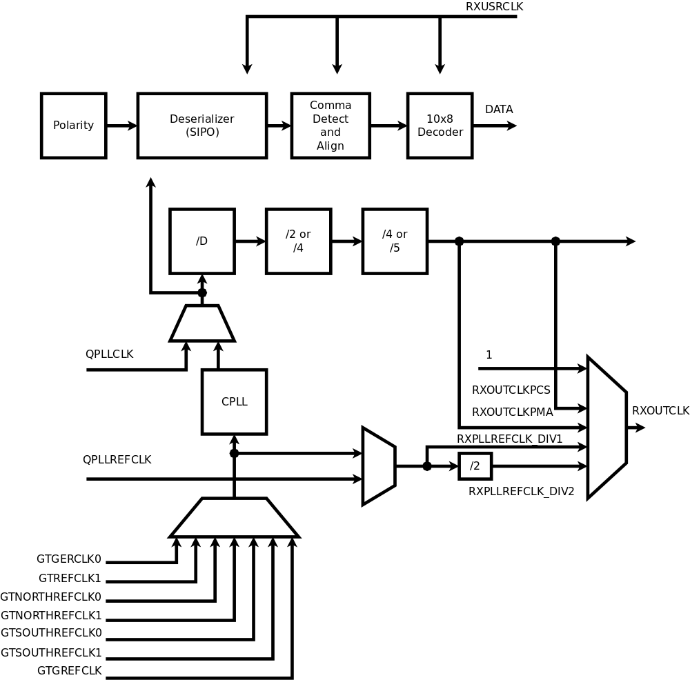
The overall design of the so called GTX_GPL is split into 4 parts, contained in a wrapper to ensure interface compatibility with the original GTX. These parts are: TX – transmitter, RX – receiver, channel clocking and common clocking.
All of the clocking scheme was based on an assumption of clocks, PLLs, and interconnects being ideal, so no setup/hold violation/metastability are expected. That itself makes the design non-synthesizable, but greatly reduces its complexity.
Receiver + Clocking
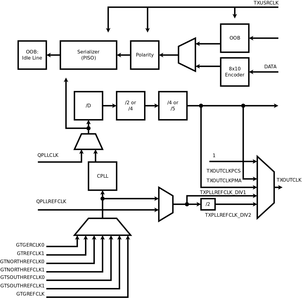
Transmitter + Clocking
Transmitter and receiver schemes are presented in the figures. Each is provided with a clocking mechanism. You can compare it to GTX’s corresponding schemes (see UG476, pages 107, 133, 149, 169). As you can see, TX and RX lack the original functional blocks. However, many of them are important only for synthesis or precise post-synthesis simulation, like phase adjustments or analog-level blocks. Some of them (like the gearbox) are excessive for SATA and implementing them can be costly.
Despite all of that, current implementation passes some basic tests when SATA parameters are turned on. Resulting waves were compared to ones received by swapping GTX_GPL with the original GTX_CHANNEL primitive as a device-under-test, and they showed more or less the same behavior.
You can access to a current version via github. It’s not necessary to clone or download the whole repository, but enough to acquire ‘GTXE2_CHANNEL.v’ file from there. This file represents a collection of all necessary modules from the repository, with GTXE2_CHANNEL as a top. After including (or linking as a lib file/source file) it in your project, the original unisims primitive GTXE2_CHANNEL.v will be overridden.
If you find some bugs during simulation in SATA context or you want some features to be implemented (within any protocol’s set-up), feel free to leave a message via comments, PM or github.
Overall, the design shall be useful for verification purposes. It allows to create a proper GPL licensed simulation verification environment which is not hard-bound to a proprietary software.