File:10353-10359-fpc-cable2.jpeg
uploaded "[[File:10353-10359-fpc-cable2.jpeg]]"
Oleg
10398
← Older revision
Revision as of 02:23, 13 November 2015
(3 intermediate revisions not shown)Line 1:
Line 1:
==10398== ==10398==
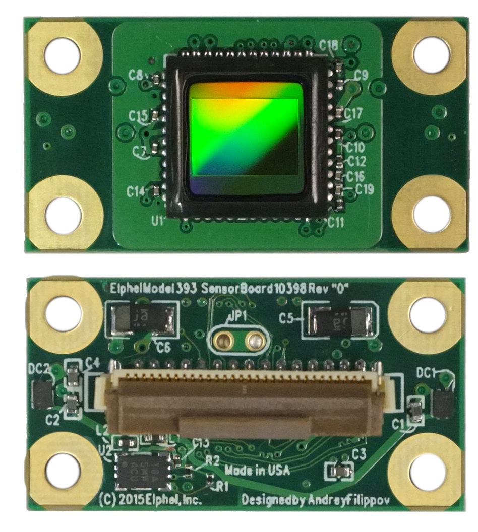
-[[Image:10398_top.png| thumb | 374px| 10398 board, top view]]+[[Image:10398_top.png|thumb|374px|10398 board, top view]]
-[[Image:10398_bottom.png| thumb | 374px| 10398 board, bottom view]]+[[Image:10398_bottom.png|thumb|374px|10398 board, bottom view]]
-10398 board is a 14MPix sensor front end (SFE) designed to work with [[10393]] camera system board. It has the same physical dimensions and the same optical format (1/2.3") as a 5MPix SFE [[10338D]].+10398 board is a 14MPix sensor front end (SFE) designed to work with [[10393]] camera system board. It has the same physical dimensions and the same optical format (1/2.3") as a 5MPix SFE [[10338D]] (15mm x 28mm).
-The 14MPix (4608H x 3288V, 1.4μm x1.4 μm) image sensor used is On Semiconductor (former Aptina) [http://www.onsemi.com/pub_link/Collateral/MT9F002-D.PDF |MT9F002]. This sensor (and 10398 SFE) uses 4-lane HiSPi serial interface running at 700 Mpbs/lane and is capable of running at 13.7 fps at full resolution (12bpp mode), or 60fps at 2304x1296 (1080p + 20% EIS). Other combinations of resolution/frame rate are possible.+The 14MPix (4608H x 3288V, 1.4μm x1.4 μm) image sensor used is On Semiconductor (former Aptina) [http://www.onsemi.com/pub_link/Collateral/MT9F002-D.PDF MT9F002]. This sensor (and 10398 SFE) uses 4-lane HiSPi serial interface running at 700 Mpbs/lane and is capable of running at 13.7 fps at full resolution (12bpp mode), or 60fps at 2304x1296 (1080p + 20% EIS). Other combinations of resolution/frame rate are possible.
-Up to 4 10398 SFE can be directly connected to [[10393]] system board and run simultaneously at full speed (880 pixels/s combined).+Up to 4 10398 SFE can be directly connected to [[10393]] system board and run simultaneously at full speed (880M pixels/s combined).
10398 SFE uses the same 30-pin flex cable connector for control (I²C, extra GPIO), differential data output (4-lane HiSPi+clock) and 3.3V power (additional 2.8V analog and 1.8V digital are generated on board). Short connections can use general purpose flex jumpers (30 conductors, 0.5mm pitch) or Elphel flex cables manufactured for the parallel interface sensors, longer connections require controlled-impedance flex cables with 100Ω differential lines. 10398 SFE uses the same 30-pin flex cable connector for control (I²C, extra GPIO), differential data output (4-lane HiSPi+clock) and 3.3V power (additional 2.8V analog and 1.8V digital are generated on board). Short connections can use general purpose flex jumpers (30 conductors, 0.5mm pitch) or Elphel flex cables manufactured for the parallel interface sensors, longer connections require controlled-impedance flex cables with 100Ω differential lines.
[[Media:10398.pdf|10398 Circuit Diagram, Parts List]] <br/> [[Media:10398_gerber.tar.gz|10398 Gerber files]] [[Media:10398.pdf|10398 Circuit Diagram, Parts List]] <br/> [[Media:10398_gerber.tar.gz|10398 Gerber files]]
Oleg
10393
More details:
← Older revision Revision as of 23:04, 12 November 2015 (4 intermediate revisions not shown)Line 20: Line 20: * microSD card slot - storage and system recovery * microSD card slot - storage and system recovery ====Interfaces==== ====Interfaces==== +[[File:Nc393 4sensors.jpeg|thumb|220px|10393 + 4 sensors]] * Gigabit ethernet * Gigabit ethernet * micro USB - system console, reboot, select boot device * micro USB - system console, reboot, select boot device Line 33: Line 34: *** carry 3.3VDC, 5VDC, USB, I<sup>2</sup>C and GPIO *** carry 3.3VDC, 5VDC, USB, I<sup>2</sup>C and GPIO *** support other extension boards ([[103695|IMU]], [[103696|GPS]]) *** support other extension boards ([[103695|IMU]], [[103696|GPS]]) + ====Other==== ====Other==== * Compressor bandwidth - up to <b>1 GPix/s</b> (e.g., processing 10MPix@100fps) * Compressor bandwidth - up to <b>1 GPix/s</b> (e.g., processing 10MPix@100fps) Line 59: Line 61: ==More details== ==More details== -[[Image:10393_bd.png|frame|[[Media:10393.pdf|10393 Circuit Diagram, Parts List, PCB layout]] [[Media:10393_gerber.tar.gz|10353 Gerber files]]]]+[[Image:10393_bd.png|thumb|400px|[[Media:10393.pdf|10393 Circuit Diagram, Parts List, PCB layout]] [[Media:10393_gerber.tar.gz|10353 Gerber files]]]] This camera system board is designed to simultaneously support multiple sensors - both with legacy parallel interface (it is directly compatible with [[10338|10338 Sensor board]] and [[10359|10359 Sensor multiplexer board]]) and with new high-speed serial interface (up to 8 lanes + clock per each port), such as [[10398 | 10398 14MPix SFE]]. Sensor ports of the 10393 can be combined to interface larger/higher speed sensors, interface supply voltage is programmable in the range of 1.35V to 2.8V. All the sensor port interface signals are routed directly to the FPGA pads (22 I/O signals on each of the 4 flex cable connectors) , so the same ports can be uses for other purposes, for example to control the motors or interface IMU of the quadcopter. This camera system board is designed to simultaneously support multiple sensors - both with legacy parallel interface (it is directly compatible with [[10338|10338 Sensor board]] and [[10359|10359 Sensor multiplexer board]]) and with new high-speed serial interface (up to 8 lanes + clock per each port), such as [[10398 | 10398 14MPix SFE]]. Sensor ports of the 10393 can be combined to interface larger/higher speed sensors, interface supply voltage is programmable in the range of 1.35V to 2.8V. All the sensor port interface signals are routed directly to the FPGA pads (22 I/O signals on each of the 4 flex cable connectors) , so the same ports can be uses for other purposes, for example to control the motors or interface IMU of the quadcopter. Oleg10393
← Older revision
Revision as of 21:43, 12 November 2015
(2 intermediate revisions not shown)Line 20:
Line 20:
* microSD card slot - storage and system recovery * microSD card slot - storage and system recovery
====Interfaces==== ====Interfaces====
+[[File:Nc393 4sensors.jpeg|thumb|220px|10393 + 4 sensors]]
* Gigabit ethernet * Gigabit ethernet
* micro USB - system console, reboot, select boot device * micro USB - system console, reboot, select boot device
Line 33:
Line 34:
*** carry 3.3VDC, 5VDC, USB, I<sup>2</sup>C and GPIO *** carry 3.3VDC, 5VDC, USB, I<sup>2</sup>C and GPIO
*** support other extension boards ([[103695|IMU]], [[103696|GPS]]) *** support other extension boards ([[103695|IMU]], [[103696|GPS]])
+
====Other==== ====Other====
* Compressor bandwidth - up to <b>1 GPix/s</b> (e.g., processing 10MPix@100fps) * Compressor bandwidth - up to <b>1 GPix/s</b> (e.g., processing 10MPix@100fps)
Oleg
File:Nc393 4sensors.jpeg
uploaded "[[File:Nc393 4sensors.jpeg]]"
Oleg
10393
← Older revision
Revision as of 21:25, 12 November 2015
(One intermediate revision not shown)Line 1:
Line 1:
+==About==
[[Image:10393_top_sm.png|frame|[[Media:10393_top.jpeg|10393 board, top view]]]] [[Image:10393_top_sm.png|frame|[[Media:10393_top.jpeg|10393 board, top view]]]]
[[Image:10393_bottom_sm.png|frame|[[Media:10393_bottom.jpeg|10393 board, bottom view]]]] [[Image:10393_bottom_sm.png|frame|[[Media:10393_bottom.jpeg|10393 board, bottom view]]]]
-[[Image:10393_bd.png|frame|[[Media:10393.pdf|10393 Circuit Diagram, Parts List, PCB layout]] [[Media:10393_gerber.tar.gz|10353 Gerber files]]]]
10393 is the system board of Elphel NC393 series camera. It will also replace [[10353|10353 board]] in [[Elphel_Eyesis4Pi|Eyesis4pi]] and other Elphel multi-sensor cameras. It has the same physical dimensions as 10353 and may be used as an upgrade to the previous camera modules. 10393 is the system board of Elphel NC393 series camera. It will also replace [[10353|10353 board]] in [[Elphel_Eyesis4Pi|Eyesis4pi]] and other Elphel multi-sensor cameras. It has the same physical dimensions as 10353 and may be used as an upgrade to the previous camera modules.
+==Overview==
+====Operating System====
+* OpenEmbedded Linux (built with [https://www.yoctoproject.org/tools-resources/projects/poky Yocto Poky])
+====Processor====
+* Xilinx Zynq 7030 SoC
+** Dual-core ARM Cortex-A9 + FPGA
+** 800MHz
+====Supported Image Sensors====
+* [http://www.onsemi.com/PowerSolutions/product.do?id=MT9P006 MT9P006] - 5MPix 1/2.5" CMOS
+* [http://www.onsemi.com/PowerSolutions/product.do?id=MT9F002 MT9F002] - 14MPix 1/2.3" CMOS
+====Memory and Storage====
+* 1.0 GB DDR3 memory - system RAM
+* 0.5 GB DDR3 memory - FPGA RAM
+* 0.5 GB NAND flash - program storage
+* microSD card slot - storage and system recovery
+====Interfaces====
+* Gigabit ethernet
+* micro USB - system console, reboot, select boot device
+* 4x sensor ports - routed to FPGA, each reconfigurable for general multi-purpose use
+* Added by [[10389|10389 Extension board]]:
+** USB2.0 (host)
+** eSATA + USB port
+** M.2 SATA port
+** External synchronization (master or slave):
+*** 2.5mm audio
+*** 4-conductor flex cable
+** 2x 10-conductor flex cable ports
+*** carry 3.3VDC, 5VDC, USB, I<sup>2</sup>C and GPIO
+*** support other extension boards ([[103695|IMU]], [[103696|GPS]])
+====Other====
+* Compressor bandwidth - up to <b>1 GPix/s</b> (e.g., processing 10MPix@100fps)
+* Image formats: JPEG, JP4, RAW (coming)
+* Wake-up on alarm
+====Power====
+* 3.3VDC
+====Dimensions====
+* 96x38 mm
+
+====SDK====
+* Firmware:
+** [https://eclipse.org Eclipse IDE] + [https://github.com/Elphel/vdt-plugin VDT-Plugin]
+** [http://www.xilinx.com/products/design-tools/vivado.html Vivado WebPACK Edition]
+** [http://iverilog.icarus.com/ IVerilog]
+** [http://gtkwave.sourceforge.net/ GTKWave]
+* Software (Kernel and Applications):
+** [https://eclipse.org Eclipse IDE]
+** [https://www.yoctoproject.org/tools-resources/projects/poky Yocto Poky]
+* Sources:
+** [https://github.com/Elphel GitHub/Elphel]
+
+====License====
+* [http://www.ohwr.org/projects/cernohl CERN OHLv1.1+]
+* [http://www.gnu.org/licenses/gpl.html GPLv3+]
+
+==More details==
+[[Image:10393_bd.png|frame|[[Media:10393.pdf|10393 Circuit Diagram, Parts List, PCB layout]] [[Media:10393_gerber.tar.gz|10353 Gerber files]]]]
This camera system board is designed to simultaneously support multiple sensors - both with legacy parallel interface (it is directly compatible with [[10338|10338 Sensor board]] and [[10359|10359 Sensor multiplexer board]]) and with new high-speed serial interface (up to 8 lanes + clock per each port), such as [[10398 | 10398 14MPix SFE]]. Sensor ports of the 10393 can be combined to interface larger/higher speed sensors, interface supply voltage is programmable in the range of 1.35V to 2.8V. All the sensor port interface signals are routed directly to the FPGA pads (22 I/O signals on each of the 4 flex cable connectors) , so the same ports can be uses for other purposes, for example to control the motors or interface IMU of the quadcopter. This camera system board is designed to simultaneously support multiple sensors - both with legacy parallel interface (it is directly compatible with [[10338|10338 Sensor board]] and [[10359|10359 Sensor multiplexer board]]) and with new high-speed serial interface (up to 8 lanes + clock per each port), such as [[10398 | 10398 14MPix SFE]]. Sensor ports of the 10393 can be combined to interface larger/higher speed sensors, interface supply voltage is programmable in the range of 1.35V to 2.8V. All the sensor port interface signals are routed directly to the FPGA pads (22 I/O signals on each of the 4 flex cable connectors) , so the same ports can be uses for other purposes, for example to control the motors or interface IMU of the quadcopter.
Oleg
10393
← Older revision
Revision as of 21:18, 12 November 2015
Line 2:
Line 2:
[[Image:10393_bottom_sm.png|frame|[[Media:10393_bottom.jpeg|10393 board, bottom view]]]] [[Image:10393_bottom_sm.png|frame|[[Media:10393_bottom.jpeg|10393 board, bottom view]]]]
[[Image:10393_bd.png|frame|[[Media:10393.pdf|10393 Circuit Diagram, Parts List, PCB layout]] [[Media:10393_gerber.tar.gz|10353 Gerber files]]]] [[Image:10393_bd.png|frame|[[Media:10393.pdf|10393 Circuit Diagram, Parts List, PCB layout]] [[Media:10393_gerber.tar.gz|10353 Gerber files]]]]
+
+==About==
10393 is the system board of Elphel NC393 series camera. It will also replace [[10353|10353 board]] in [[Elphel_Eyesis4Pi|Eyesis4pi]] and other Elphel multi-sensor cameras. It has the same physical dimensions as 10353 and may be used as an upgrade to the previous camera modules. 10393 is the system board of Elphel NC393 series camera. It will also replace [[10353|10353 board]] in [[Elphel_Eyesis4Pi|Eyesis4pi]] and other Elphel multi-sensor cameras. It has the same physical dimensions as 10353 and may be used as an upgrade to the previous camera modules.
+==Overview==
+====Operating System====
+* OpenEmbedded Linux (built with [https://www.yoctoproject.org/tools-resources/projects/poky Yocto Poky])
+====Processor====
+* Xilinx Zynq 7030 SoC
+** Dual-core ARM Cortex-A9 + FPGA
+** 800MHz
+====Supported Image Sensors====
+* [http://www.onsemi.com/PowerSolutions/product.do?id=MT9P006 MT9P006] - 5MPix 1/2.5" CMOS
+* [http://www.onsemi.com/PowerSolutions/product.do?id=MT9F002 MT9F002] - 14MPix 1/2.3" CMOS
+====Memory and Storage====
+* 1.0 GB DDR3 memory - system RAM
+* 0.5 GB DDR3 memory - FPGA RAM
+* 0.5 GB NAND flash - program storage
+* microSD card slot - storage and system recovery
+====Interfaces====
+* Gigabit ethernet
+* micro USB - system console, reboot, select boot device
+* 4x sensor ports - routed to FPGA, each reconfigurable for general multi-purpose use
+* Added by [[10389|10389 Extension board]]:
+** USB2.0 (host)
+** eSATA + USB port
+** M.2 SATA port
+** External synchronization (master or slave):
+*** 2.5mm audio
+*** 4-conductor flex cable
+** 2x 10-conductor flex cable ports
+*** carry 3.3VDC, 5VDC, USB, I<sup>2</sup>C and GPIO
+*** support other extension boards ([[103695|IMU]], [[103696|GPS]])
+====Other====
+* Compressor bandwidth - up to <b>1 GPix/s</b> (e.g., processing 10MPix@100fps)
+* Image formats: JPEG, JP4, RAW (coming)
+* Wake-up on alarm
+====Power====
+* 3.3VDC
+====Dimensions====
+* 96x38 mm
+
+====SDK====
+* Firmware:
+** [https://eclipse.org Eclipse IDE] + [https://github.com/Elphel/vdt-plugin VDT-Plugin]
+** [http://www.xilinx.com/products/design-tools/vivado.html Vivado WebPACK Edition]
+** [http://iverilog.icarus.com/ IVerilog]
+** [http://gtkwave.sourceforge.net/ GTKWave]
+* Software (Kernel and Applications):
+** [https://eclipse.org Eclipse IDE]
+** [https://www.yoctoproject.org/tools-resources/projects/poky Yocto Poky]
+* Sources:
+** [https://github.com/Elphel GitHub/Elphel]
+
+====License====
+* [http://www.ohwr.org/projects/cernohl CERN OHLv1.1+]
+* [http://www.gnu.org/licenses/gpl.html GPLv3+]
+
+
+
+==More details==
This camera system board is designed to simultaneously support multiple sensors - both with legacy parallel interface (it is directly compatible with [[10338|10338 Sensor board]] and [[10359|10359 Sensor multiplexer board]]) and with new high-speed serial interface (up to 8 lanes + clock per each port), such as [[10398 | 10398 14MPix SFE]]. Sensor ports of the 10393 can be combined to interface larger/higher speed sensors, interface supply voltage is programmable in the range of 1.35V to 2.8V. All the sensor port interface signals are routed directly to the FPGA pads (22 I/O signals on each of the 4 flex cable connectors) , so the same ports can be uses for other purposes, for example to control the motors or interface IMU of the quadcopter. This camera system board is designed to simultaneously support multiple sensors - both with legacy parallel interface (it is directly compatible with [[10338|10338 Sensor board]] and [[10359|10359 Sensor multiplexer board]]) and with new high-speed serial interface (up to 8 lanes + clock per each port), such as [[10398 | 10398 14MPix SFE]]. Sensor ports of the 10393 can be combined to interface larger/higher speed sensors, interface supply voltage is programmable in the range of 1.35V to 2.8V. All the sensor port interface signals are routed directly to the FPGA pads (22 I/O signals on each of the 4 flex cable connectors) , so the same ports can be uses for other purposes, for example to control the motors or interface IMU of the quadcopter.
Oleg
NC393 progress update: 14MPix Sensor Front End is up and running
10398 Sensor Front End with 14MPix MT9F002
Sensors (ON Semiconductor MT9F002) and blank PCBs arrived in time and so I was able to hand-assemble two 10398 boards and start testing them. I had some minor problems getting data output from the first board, but it turned out to be just my bad soldering of the sensor, the second board worked immediately. To my surprise I did not have any problems with HiSPi decoder that I simulated using the sensor model I wrote myself from the documentation, so the color bar test pattern appeared almost immediately, followed by the real acquired images. I kept most of the sensor settings unmodified from the default values, just selected the correct PLL multiplier, output signal levels (1.8V HiVCM – compatible with the FPGA) and packetized format, the only other registers I had to adjust manually were exposure and color analog gains.
As it was reasonable to expect, sensitivity of the 14MPix sensor is lower than that of the 5MPix MT9P006 – our initial estimate is that it is 4 times lower, but this needs more careful measurements to find out exposure required for pixel saturation with the same illumination. Analog channel gains for both sensors we set slightly higher than minimal ones for the saturation, but such rough measurements could easily miss a factor of 1.5. MT9F002 offers more controls over the signal chain gains, but any (even analog) gain in the chain that boosts signal above the minimal needed for saturation proportionally reduces used “well capacity”, while I expect the Full Well Capacity (FWC) is already not very high for the 1.4μm x1.4 μm pixel sensor. And decrease in the number of electrons stored in a pixel accordingly increases the relative shot noise that reveals itself in the highlight areas. We will need to accurately measure FWC of the MT9F002 and have better sensitivity comparison, including that of the binned mode, but I expect to find out that 5MPix sensor are not obsolete yet and for some applications may still have advantages over the newer sensors.
Image acquired with 5 MPix MT9P006 sensor, 1/2000 s
Image acquired with 14MPix MT9F002 sensor, 1/500 s
Both sensors used identical f=4.5mm F3.0 lenses, the 5MPix one lens is precisely adjusted during calibration, the lens of the 14MPix sensor is just attached and focused by hand using the lens thread, no tilt correction was performed. Both images are saved at 100% JPEG quality (lossless compression) to eliminate compression artifacts, both used in-camera simple 3×3 demosaic algorithm. The 14 MPix image has visible checkerboard pattern caused by the difference of the 2 green values (green in red row, and green in the blue row). I’ll check that it is not caused by some FPGA code bug I might introduce (save as raw image and do de-bayer on a host computer), but it may also be caused by pixel cross-talk in the sensor. In any case it is possible to compensate or at least significantly reduce in the output data.
MT9F002 transmits data over 5 differential 100Ω pairs: 1 clock pair and 4 data lanes. For the initial tests I used our regular 70mm flex cable used for the parallel interface sensors, and just soldered 5 of 100Ω resistors to the contacts at the camera side end. It did work and I did not even have to do any timing adjustments of the differential lanes. We’ll do such adjustments in the future to get to the centers of the data windows – both the sensor and the FPGA code have provisions for that. The physical 100Ω load resistors were needed as it turned out that Xilinx Zynq has on-chip differential termination only for the 2.5V (or higher) supply voltages on the regular (not “high performance”) I/Os and this application uses 1.8V interface power – I missed this part of documentation and assumed that all the differential inputs have possibility to turn on differential termination. 660 Mbps/lane data rate is not too high and I expect that it will be possible to use short cables with no load resistors at all, adding such resistors to the 10393 board is not an option as it has to work with both serial and parallel sensor interfaces. Simultaneously we designed and placed an order for dedicated flex cables 150mm long, if that will work out we’ll try longer (450mm) controlled impedance cables.
File:10398.pdf
deleted "[[File:10398.pdf]]" Deleted old revision 20151112064946!10398.pdf: obsolete
Andrey.filippov10398
← Older revision
Revision as of 03:15, 12 November 2015
(One intermediate revision not shown)Line 6:
Line 6:
The 14MPix (4608H x 3288V, 1.4μm x1.4 μm) image sensor used is On Semiconductor (former Aptina) [http://www.onsemi.com/pub_link/Collateral/MT9F002-D.PDF |MT9F002]. This sensor (and 10398 SFE) uses 4-lane HiSPi serial interface running at 700 Mpbs/lane and is capable of running at 13.7 fps at full resolution (12bpp mode), or 60fps at 2304x1296 (1080p + 20% EIS). Other combinations of resolution/frame rate are possible. The 14MPix (4608H x 3288V, 1.4μm x1.4 μm) image sensor used is On Semiconductor (former Aptina) [http://www.onsemi.com/pub_link/Collateral/MT9F002-D.PDF |MT9F002]. This sensor (and 10398 SFE) uses 4-lane HiSPi serial interface running at 700 Mpbs/lane and is capable of running at 13.7 fps at full resolution (12bpp mode), or 60fps at 2304x1296 (1080p + 20% EIS). Other combinations of resolution/frame rate are possible.
+
+Up to 4 10398 SFE can be directly connected to [[10393]] system board and run simultaneously at full speed (880 pixels/s combined).
10398 SFE uses the same 30-pin flex cable connector for control (I²C, extra GPIO), differential data output (4-lane HiSPi+clock) and 3.3V power (additional 2.8V analog and 1.8V digital are generated on board). Short connections can use general purpose flex jumpers (30 conductors, 0.5mm pitch) or Elphel flex cables manufactured for the parallel interface sensors, longer connections require controlled-impedance flex cables with 100Ω differential lines. 10398 SFE uses the same 30-pin flex cable connector for control (I²C, extra GPIO), differential data output (4-lane HiSPi+clock) and 3.3V power (additional 2.8V analog and 1.8V digital are generated on board). Short connections can use general purpose flex jumpers (30 conductors, 0.5mm pitch) or Elphel flex cables manufactured for the parallel interface sensors, longer connections require controlled-impedance flex cables with 100Ω differential lines.
-[[Media:10398.jpeg|10398 Circuit Diagram, Parts List]] <br/> [[Media:10398_gerber.tar.gz|10398 Gerber files]]+[[Media:10398.pdf|10398 Circuit Diagram, Parts List]] <br/> [[Media:10398_gerber.tar.gz|10398 Gerber files]]
Andrey.filippov
10393
← Older revision
Revision as of 03:04, 12 November 2015
(One intermediate revision not shown)Line 4:
Line 4:
10393 is the system board of Elphel NC393 series camera. It will also replace [[10353|10353 board]] in [[Elphel_Eyesis4Pi|Eyesis4pi]] and other Elphel multi-sensor cameras. It has the same physical dimensions as 10353 and may be used as an upgrade to the previous camera modules. 10393 is the system board of Elphel NC393 series camera. It will also replace [[10353|10353 board]] in [[Elphel_Eyesis4Pi|Eyesis4pi]] and other Elphel multi-sensor cameras. It has the same physical dimensions as 10353 and may be used as an upgrade to the previous camera modules.
-This camera system board is designed to simultaneously support multiple sensors - both with legacy parallel interface (it is directly compatible with [[10338|10338 Sensor board]] and [[10359|10359 Sensor multiplexer board]]) and with new high-speed serial interface (up to 8 lanes + clock per each port). Sensor ports of the 10393 can be combined to interface larger/higher speed sensors, interface supply voltage is programmable in the range of 1.35V to 2.8V. All the sensor port interface signals are routed directly to the FPGA pads (22 I/O signals on each of the 4 flex cable connectors) , so the same ports can be uses for other purposes, for example to control the motors or interface IMU of the quadcopter.+This camera system board is designed to simultaneously support multiple sensors - both with legacy parallel interface (it is directly compatible with [[10338|10338 Sensor board]] and [[10359|10359 Sensor multiplexer board]]) and with new high-speed serial interface (up to 8 lanes + clock per each port), such as [[10398 | 10398 14MPix SFE]]. Sensor ports of the 10393 can be combined to interface larger/higher speed sensors, interface supply voltage is programmable in the range of 1.35V to 2.8V. All the sensor port interface signals are routed directly to the FPGA pads (22 I/O signals on each of the 4 flex cable connectors) , so the same ports can be uses for other purposes, for example to control the motors or interface IMU of the quadcopter.
Block diagram below shows major parts and I/O ports of the 10393 board. Left edge of the diagram corresponds to the sensor connections, right one - to the camera back panel with external connectors, top and bottom contain inter-board connections: Block diagram below shows major parts and I/O ports of the 10393 board. Left edge of the diagram corresponds to the sensor connections, right one - to the camera back panel with external connectors, top and bottom contain inter-board connections:
Andrey.filippov
10398
← Older revision
Revision as of 03:02, 12 November 2015
(One intermediate revision not shown)Line 1:
Line 1:
==10398== ==10398==
-[[Image:10398.png | frame|[[Media:10398.pdf|10398 Circuit Diagram, Parts List]] <br/> [[Media:10398_gerber.tar.gz|10398 Gerber files]]]]+[[Image:10398_top.png| thumb | 374px| 10398 board, top view]]
+[[Image:10398_bottom.png| thumb | 374px| 10398 board, bottom view]]
+
+10398 board is a 14MPix sensor front end (SFE) designed to work with [[10393]] camera system board. It has the same physical dimensions and the same optical format (1/2.3") as a 5MPix SFE [[10338D]].
+
+The 14MPix (4608H x 3288V, 1.4μm x1.4 μm) image sensor used is On Semiconductor (former Aptina) [http://www.onsemi.com/pub_link/Collateral/MT9F002-D.PDF |MT9F002]. This sensor (and 10398 SFE) uses 4-lane HiSPi serial interface running at 700 Mpbs/lane and is capable of running at 13.7 fps at full resolution (12bpp mode), or 60fps at 2304x1296 (1080p + 20% EIS). Other combinations of resolution/frame rate are possible.
+
+10398 SFE uses the same 30-pin flex cable connector for control (I²C, extra GPIO), differential data output (4-lane HiSPi+clock) and 3.3V power (additional 2.8V analog and 1.8V digital are generated on board). Short connections can use general purpose flex jumpers (30 conductors, 0.5mm pitch) or Elphel flex cables manufactured for the parallel interface sensors, longer connections require controlled-impedance flex cables with 100Ω differential lines.
+
+[[Media:10398.jpeg|10398 Circuit Diagram, Parts List]] <br/> [[Media:10398_gerber.tar.gz|10398 Gerber files]]
Andrey.filippov
File:10398.jpeg
uploaded "[[File:10398.jpeg]]"
Andrey.filippov
10398
Created page with "==10398== 10398 Circuit Diagram, Parts List <br/> 10398 Gerber files]]"
New page
==10398==[[Image:10398.png | frame|[[Media:10398.pdf|10398 Circuit Diagram, Parts List]] <br/> [[Media:10398_gerber.tar.gz|10398 Gerber files]]]] Andrey.filippov
File:10398.png
uploaded "[[File:10398.png]]"
Andrey.filippovFile:10398 bottom.png
uploaded "[[File:10398 bottom.png]]"
Andrey.filippov
File:10393 bottom.jpeg
uploaded a new version of "[[File:10393 bottom.jpeg]]"
Oleg
NC393 progress update: one gigapixel per second (12x faster than NC353)
All the PCBs for the new camera: 10393, 10389 and 10385 are modified to rev “A”, we already received the new boards from the factory and now are waiting for the first production batch to be build. The PCB changes are minor, just moving connectors away from the board edge to simplify mechanical design and improve thermal contact of the heat sink plate to the camera body. Additionally the 10389A got m2 connector instead of the mSATA to accommodate modern SSD.
While waiting for the production we designed a new sensor board (10398) that has exactly the same dimensions, same image sensor format as the current 10338E and so it is compatible with the hardware for the calibrated sensor front ends we use in photogrammetric cameras. The difference is that this MT9F002 is a 14 MPix device and has high-speed serial interface instead of the legacy parallel one. We expect to get the new boards and the sensors next week and will immediately start working with this new hardware.
In preparation for the faster sensors I started to work on the FPGA code to make it ready for the new devices. We planned to use modern sensors with the serial interfaces from the very beginning of the new camera design, so the hardware accommodates up to 8 differential data lanes plus a clock pair in addition to the I²C and several control signals. One obviously required part is the support for Aptina HiSPi (High Speed Serial Pixel) interface that in case of MT9F002 uses 4 differential data lanes, each running at 660 Mbps – in 12-bit mode that corresponds to 220 MPix/s. Until we’ll get the actual sensors I could only simulate receiving of the HiSPi data using the sensor model written ourselves following the interface documentation. I’ll need yet to make sure I understood the documentation correctly and the sensor will produce output similar to what we modeled.
The sensor interface is not the only piece of the code that needed changes, I also had to increase significantly the bandwidth of the FPGA signal processing and to modify the I²C sequencer to support 2-byte register addresses.
Data that FPGA receives from the sensor passes through the several clock domains until it is stored in the system memory as a sequence of compressed JPEG/JP4 frames:
- Sensor data in each channel enters FPGA at a pixel clock rate, and subsequently passes through vignetting correction/scaling module, gamma conversion module and histogram calculation modules. This chain output is buffered before crossing to the memory clock domain.
- Multichannel DDR3 memory controller records sensor data in line-scan order and later retrieves it in overlapping (for JPEG) or non-overlapping (for JP4) square tiles.
- Data tiles retrieved from the external DDR3 memory are sent to the compressor clock domain to be processed with JPEG algorithm. In color JPEG mode compressor bandwidth has to be 1.5 higher than the pixel rate, as for 4:2:0 encoding each 16×16 pixels macroblock generate 6 of the 8×8 image blocks – 4 for Y (intensity) and 2 – for color components. In JP4 mode when the de-mosaic algorithm runs on the host computer the compressor clock rate equals the pixel rate.
- Last clock domain is 150MHz used by the AXI interface that operates in 64-bit parallel mode and transfers the compressed data to the system memory.
Two of these domains used double clock rate for some of the processing stages – histograms calculation in the pixel clock domain and Huffman encoder/bit stuffer in the compressor. In the previous NC353 camera pixel clock rate was 96MHz (192 MHz for double rate) and compressor rate was 80MHz (160MHz for double rate). The sensor/compressor clock rates difference reflects the fact that the sensor data output is not uniform (it pauses during inactive lines) and the compressor can process the frame at a steady rate.
MT9F002 image sensor has the output pixel rate of 220MPix/s with the average (over the full frame) rate of 198MPix/s. Using double rate clocks (440MHz for the sensor channel and 400MHz for the compressor) would be rather difficult on Zynq, so I needed first to eliminate such clocks in the design. It was possible to implement and test this modification with the existing sensor, and now it is done – four of the camera compressors each run at 250 MHz (even on “-1″, or “slow” speed grade silicon) making it total of 1GPix/sec. It does not need to have 4 separate sensors running simultaneously – a single high speed imager can provide data for all 4 compressors, each processing every 4-th frame as each image is processed independently.
At this time the memory controller will be a bottleneck when running all four MT9F002 sensors simultaneously as it currently provides only 1600MB/s bandwidth that may be marginally sufficient for four MT9F002 sensor channels and 4 compressor channels each requiring 200MB/s (bandwidth overhead is just a few percent). I am sure it will be possible to optimize the memory controller code to run at higher rate to match the compressors. We already identified which parts of the memory controller need to be modified to support 1.5x clock increase to the total of 2400MB/s. And as the production NC393 camera will have higher speed grade SoC there will be an extra 20% performance increase for the same code. That will provide bandwidth sufficient not just to run 4 sensors at full speed and compress the output data, but to do some other image manipulation at the same time.
Compared to the previous Elphel NC353 camera the new NC393 prototype already is tested to have 12x higher compressor bandwidth (4 channels instead of one and 250MPix/s instead of 80MPix/s), we plan to have the actual sensor with a full data processing chain results soon.
10338D
← Older revision
Revision as of 19:58, 3 November 2015
Line 2:
Line 2:
[[Image:10338d.jpeg|frame|[[Media:10338d.jpeg|10338 board, rev D and E]]]] [[Image:10338d.jpeg|frame|[[Media:10338d.jpeg|10338 board, rev D and E]]]]
[[Image:10338bd.png|frame|[[Media:10338d.pdf|10338D Circuit Diagram, PCB layout]] <br/> [[Media:10338d_gerber.tar.gz|10338 rev D Gerber files]]]] [[Image:10338bd.png|frame|[[Media:10338d.pdf|10338D Circuit Diagram, PCB layout]] <br/> [[Media:10338d_gerber.tar.gz|10338 rev D Gerber files]]]]
-10338D is a modification of the earlier [[10338]] board designed to interface Aptina (before Micron) MT9P031/MT9P001 5MPix (2592x1944) sensor to [[353|Elphel Model 353/363 Cameras]]. This board has smaller physical size (15mm x 28mm) to fit in multisensor panoramic setups.+10338D/10338E is a modification of the earlier [[10338]] board designed to interface Aptina (before Micron) MT9P031/MT9P001/MT9P006 5MPix (2592x1944) sensor to [[353|Elphel Model 353 Cameras]]. This board has smaller physical size (15mm x 28mm) to fit in multisensor panoramic setups.
Connectors: Connectors:
* 30-pin flex cable connector (J1) for data and power. * 30-pin flex cable connector (J1) for data and power.
Andrey.filippov
User:Saint17
Blanked the page
← Older revision Revision as of 09:53, 29 October 2015 Line 1: Line 1: -Jeff Leach -*leach17 at gmail.com - -"There can be only one!" Saint17