Open Hardware Lens for Eyesis4π camera
Elphel has embarked on a new project, somewhat different from our main field of designing digital cameras, but closely related to the camera applications and aimed to further improve image quality of Eyesis4π camera. Eyesis4π is a high resolution full-sphere panoramic and stereophotogrammetric camera. It is a tiled multi-sensor system with a single sensor’s format of 1/2.5″. The specific requirement of such system is uniform angular resolution, since there is no center in a panoramic image.
Current lens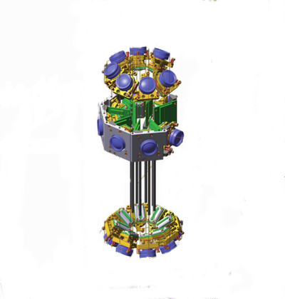
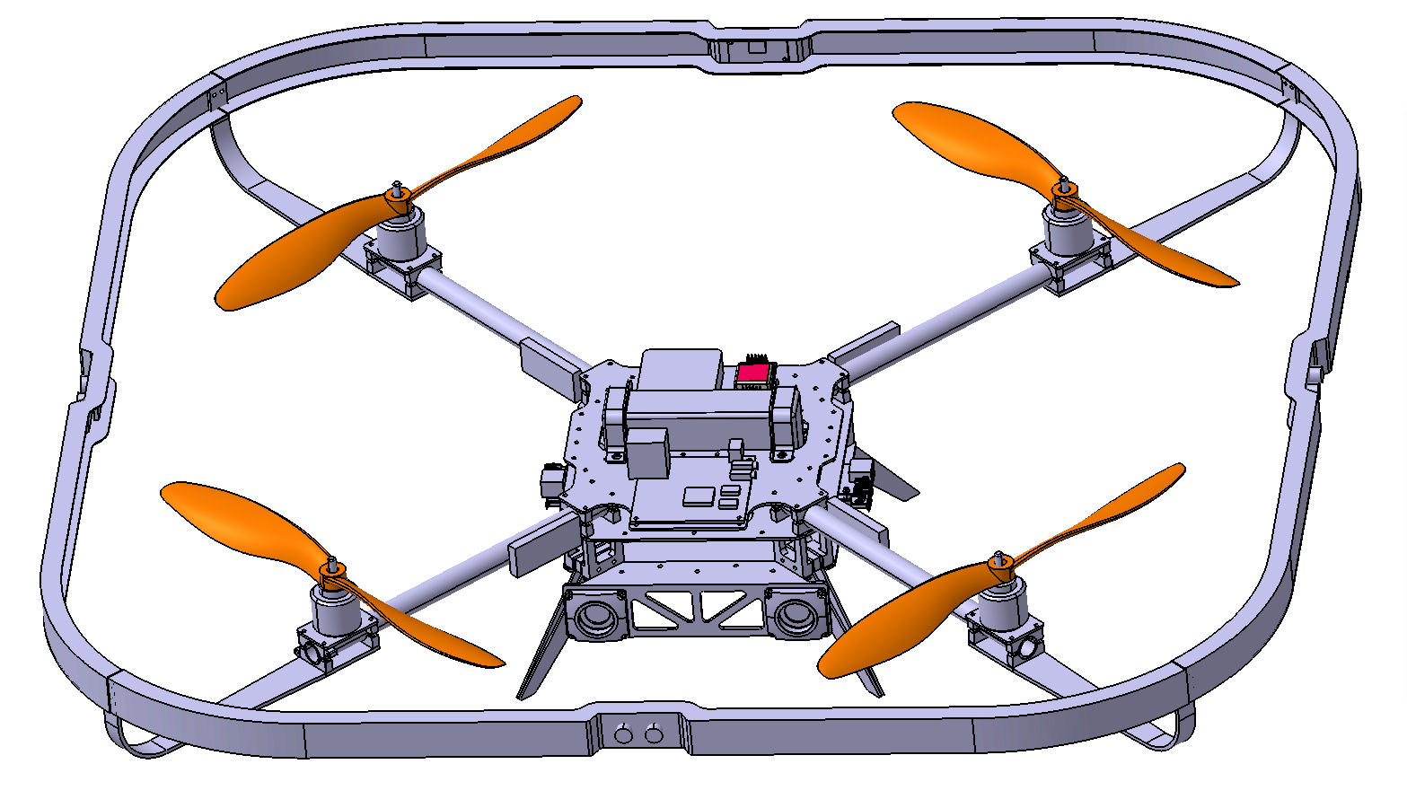
Fig.1. Eyesis4π modules layout
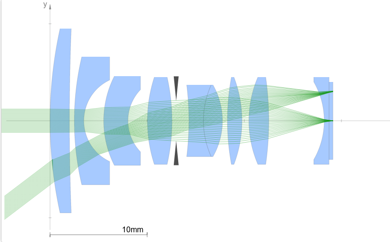
Lens selection for the camera was dictated by small form factor among other parameters and after testing a dozen of different lenses we have selected N125B04518IR, by Evetar, to be used in Eyesis4π panoramic camera. It is M12 mount (also called board lens), EFL=4.5mm, F/1.8 lens with the same 1/2.5″ format as camera’s sensor. This sensor is perfected by volume production and wide use in security and machine vision applications, which contributed to it’s high performance at a relatively low price. At the same time the price-quality balance for board lenses has mostly shifted to the lower price, and while these lenses provide good quality in the center of the image the resolution in the corners is lower and aberrations are worse. Each lens of the same model is slightly different from another, it’s overall resolution, resolution in the corners, and aberrations vary, so we have developed a more or less universal method to measure the optical parameters of the sensor-lens module that allows us to select the best lenses from a received batch. This helped us to formulate quantitative parameters to compare lens performance for our application. We have also researched other options. For example, there are compact lenses for smaller formats (used in smartphones) but most, if not all of them are designed to be integrated with the device. On the consumer cameras side better lenses are mostly designed for formats of at least 3/4″. C-mount lenses we use with other Elphel camera models are too large for Eyesis4π panoramic camera sensor-lens module layout.
Lens with high resolution over the Full Field of ViewIn panoramic application and other multi-sensor tiled cameras we are designing the center can be set anywhere and none of the board lenses (and other lenses) we have tested could provide the desirable uniform angular resolution. Thus there is a strong interest to have the lens designed in response to panoramic application requirements. Our first approach was to order custom design from lens manufacturers, but it proved to be rather difficult to specify the lens parameters, based on a standard specifications list we were offered to fill out.
The following table describes basic parameters for the initial lens design:
Parameter
Description
Mount
S-mount (M12x0.5)
Size
compact (fit in the barrel of the current lens)
Format
1/2.5"
Field of View
V: 51°, H: 65°, D: 77°
F#
f/1.8
EFL
4-4.5 mm (maybe 4.8)
Distortion
barrel type
Field Curvature
undercorrected (a field flattener will be used)
Aberrations
as low as possible
The designed lens will be subjected to the tests similar to the ones we use in actual camera calibration before it is manufactured. This way we can simulate the virtual optical design and make corrections based on it’s performance, to ensure that the designed lens satisfies our requirements before we even have the prototype. To be able to do that we realized that we need to be involved in the lens design process much more then just provide the manufacturer our list of specifications. Not having an optical engineer on board (although Andrey had majored in Optics at Moscow Institute for Physics and Technology, but worked only with laser components, and has no actual experience of lens design) we decided to get professional help from Optics For Hire with initial lens design and meanwhile getting familiar with optical design software (OSLO 6.6) – trying to create an error (merit) function that formalizes our requirements. In short, the goal is to minimize the RMS of squared spot sizes (averaging 4th power) over the full field of view taking into account the pixel’s spectral range. Right now we are trying to implement custom operands for minimization using OSLO software.
Fig.2 Online demo snapshot
As always with Elphel developments the lens design will be published under CERN Open Hardware License v1.2 and available on github – some early files are already there. We would like to invite feedback from people who are experienced in optical design to help us to find new solutions and avoid mistakes. To make it easier to participate in our efforts we are working on the online demonstration page that helps to visualize optical designs created in Zemax and OSLO. Once the lens design is finished it will be measured using Elphel set-up and software and measurement results will be also published. Other developers can use this project to create derivative designs , optimized for other applications and lens manufacturers can produce this lens as is, according to the freedoms of CERN OHL.
Links- Eyesis4π
- Lens measurement and correction technique
- Optical Design Viewer: online, github
- Optics For Hire company – Optical Design Consultants for Custom Lens Design
- Initial optical design files
DDR3 Memory Interface on Xilinx Zynq SOC – Free Software Compatible
External memory controller is an important part of many FPGA-centered designs, it is true for Elphel cameras too. When I was working on the board design for NC393 I tried to verify inteface pinout using the code output from the MIG (Memory Interface Generator) module. I was planning to use MIG code as a reference design and customize it for application in the camera, adding more functionality to our previous designs. Memory interface is a rather intimate part of the design where FPGA approach can shine it all its glory – advance knowledge of the types of needed memory transactions (in contrast with the general CPU system memory) helps to increase performance by planning bank and address sequences, crafting memory mapping to utilize close to 100% of the bus bandwidth.
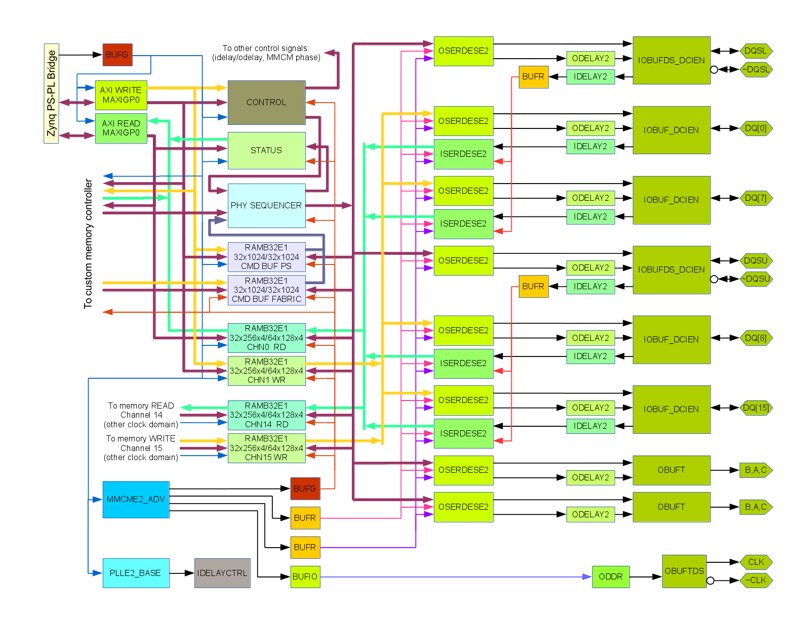
Fig. 1. DDR3 memory controller block diagram, source code at https://github.com/Elphel/eddr3
That was my original plan, but MIG code used 6 undocumented modules (PHASER_*,PHY_CONTROL) and four more (ISERDESE2,OSERDESE2,IN_FIFO and OUT_FIFO) that are only partially documented and the source code of the simulation modules is not available to Xilinx users.
This means that MIG as it is currently provided by Xilinx does not satisfy our requirements. It would prevent our customers from simulating Elphel code with Free Software tools, and it also would not allow us to develop efficient code ourselves. Developing HDL code, troubleshooting complex cases through simulation is a rather challenging task already, guessing what is going on inside the “black boxes” without the possibility to at least add some debug output there – it would be a nightmare. Why does the signal differs from what I expected – is it one of my stupid assumptions that are wrong in this case? Did I understand documentation incorrectly? Or is there just a bug in that secret no-source-code module? I browsed the Internet support forums and found that yes, there are in fact cases where users have questions about the simulation of the encrypted modules but I could not find clear answers to them. And it is understandable – it is usually difficult to help with the design made by somebody else, especially when that encrypted black box is connected to the customer code that differs from what black box developers had in mind themselves.
Does that mean that Zynq SOC is completely useless for Elphel projects?Efficient connection to the dedicated (not shared with the CPU) high performance memory is a strict requirement for Elphel products and Xilinx FPGA were always very instrumental in achieving this goal. Through more than a decade of developing cameras based on Xilinx programmable logic our cameras used SDR, then DDR and later DDR2 memory devices. After discovering that while advancing silicon technology Xilinx made a step back in the quality of the documentation and simulation support I analyzed the set of still usable modules and features of this new device to see if they alone are sufficient for our requirements.
The most important are serializer, deserializer and programmable delay elements (in both input and output directions) on each I/O pin connected to the memory device, and Xilinx Zynq does provide them.
The OSERDES2 and ISERDESE2 (serializer and deserializer modules in Xilinx Zynq) can not be simulated with Free Software tools directly as they depend on encrypted code, but their functionality (without undocumented MEMORY_DDR3 mode) matches that of Xilinx Virtex 6 devices. So with the simple wrapper modules that switch between the *SERDESE2 for synthesis with Xilinx tools and *SERDESE1 for simulation with Icarus Verilog simulator that problem was solved.
Input/output delay modules have their HDL source available and did not cause any simulation problems, so the minimal requirements were met and the project goals seemed possible to achieve.
DDR3 memory interface requirementsLooking at the Xilinx MIG implementation I compared it with our requirements and I’ve got an impression it tried to be the single universal solution for every possible application. I do not agree with such approach that contradicts the very essence of the FPGA solutions – possibility to generate “hardware” that best suits the custom application. Some universal high-level hard modules enhance bare FPGA fabric – such elements as RAM blocks, DSP, CPU – these units being specialized lost some of their flexibility (compared to than arbitrary HDL code) but became adopted by the industry and users as they offer high performance while maintaining reasonable universality – same modules can be reused in numerous applications developed by users. The lack of possibility to modify hard modules beyond provided configurable options comes as understandable price for performance – these limitations are imposed by the nature of the technology, not by the bad (or good – trying to keep inexperienced developers away from the dangers of the unrestricted FPGA design) will of the vendors.
Below is the table that compares our requirements (and acceptable limitations) of the DDR3 memory interface in comparison with Xilinx MIG solution.
Feature comparison table Feature MIG eddr3 notes Usable banks HP,HR HP only HR I/O do not support output delays and limit DCI Data width any 16 bits Data width can be manually modified Multi-rank support yes no Not required for most applications FBG484 single bank no yes MIG does not allow 256Mx16 memory use one bank in FBG484 package Access type any block oriented Overlapping between accesses may may be disregarded R/W activity on-the-fly pre-calculated Bank mapping, access sequences pre-calculated in advance Initialization, leveling hardware software Infrequent procedures implemented in software Undocumented features yes no Difficult to debug the code Encrypted modules yes no Impossible to simulate with Free Software tools, difficult to debug License proprietary GNU GPLv3.0+ Proprietary license complicates distribution of derivative code Usable I/O banksAccepting HR or “high (voltage) range” banks for memory interfacing lead MIG to sacrifice the ODELAYE2 blocks that are available in HP (“high performance”) banks only. And we did not have this limitation, as the DDR3 chip was already connected to HP bank. I believe it is true for other designs too – it makes sense do follow the bank specialization and use memory with HP banks and reserve HR for other application (like I/O) where the higher voltage range is actually needed.
Block accesses onlyAnother consideration is that having abundance of 32Kb block memory resources in the FPGA and parallel processing nature of the programmable logic, the small memory accesses are not likely, many applications do not need to bother with reduced burst sizes, data byte masking or even back-to-back reads and writes. In our applications we use 1/4 of the BRAM size transfers in most cases (1/4 comes from having a 4-page buffer at each channel to implement simple 2-level prioritizing between multiple channels. Block access does not have to be limited to memory pages – it can be any large predefined sequences of data transfer.
Hardware vs software implementation of infrequent actionsMIG feature that I think leads to unneeded complication – everything is done in “hardware”, even write leveling and temperature compensation from the on-chip temperature sensor. I was once impressed by the circuit diagram of Apple ][ computer, and learned a lesson that you do not need to waste special hardware resources on what easily can be done in software without significant sacrifice of performance. Especially in the case of a SOC like Zynq where a high-performance dual-core processor is available. Algorithms that need to run once at start-up and very infrequently during operation (temperature correction) can easily be implemented in software. The memory controller implemented in PL is initialized when the system is fully loaded, so initialization and training can be performed when the full software is available, it is not as system memory that has to be operational from the early boot stage.
Computation of the access sequences in advanceWhen dealing with the multi-channel block access (blocks do not need to be the same size and shape) in the camera, it is acceptable to have an extra latency comparable to the block read/write time, that allowed to simplify the design (and make it more flexible at the same time) by splitting generation and execution of the block access sequences in two separate processes. The physical interface sequencer reads the commands, memory addresses and control signals (as well as channel buffer read/write enable from the block memory, the sequence data is prepared in advance from 2 sources: custom PL circuitry that calculates the next block access sequence and loaded directly by the software over AXI channel (refresh, calibrate ZQ, write leveling and other delay measurement/adjustment sequences)
No multi-rankAnother simplification - I did not plan to use multi-rank systems, supplementing FPGA with just one (or several, but just to increase data width/bandwidth, not the depth/capacity) high performance memory chip is a most common configuration. Internal data paths of the programmable logic have so much higher bandwidth than the connection to an external memory, that when several memory chips are used they are usually connected to achieve the highest possible bandwidth. Of course, these considerations are usually, but not always valid. And the FPGA are very good for creating custom solutions for particular cases, not just "one size fits all".
DDR3 Interface ImplementationFig. 1 shows simplified block diagram of the eddr3 project module. It uses just one block (HP34) for interfacing 512M x 16 DDR3 memory with pinout following Xilinx recommendations for MIG. There are two identical byte lanes each having 8 bidirectional data signals running in DDR mode (DQ[0]..DQ[7] and DQ[8]..DQ[15] – only two bits per lane are shown on the diagram), one bidirectional differential DQS. There is also data mask (DM) signal in each byte lane – it is similar to DQ without input signal, and while it is supported in the physical level of the interface, it is not currently used on a higher level of the controller. There is also a differential driver for the memory clock input (CLK,~CLK) and address/command signals that are output only and run in SDR mode at the clock rate.
I/O portsData bit I/O buffers (IOBUF_DCIEN modules) are directly connected to the I/O pads produce read data outputs feeding IDELAYE2 modules, have data inputs for the write data coming form ODELAYE2 modules, output tristate control and DCI enable inputs. There is only one output delay unit per bit, so tristate control has to come directly from the OSERDESE2 module, but that is OK as the it is still possible to meet the memory requirements when controlling tristate at clock half-period granularity, even when switching between read and write commands. But in the block-oriented memory access in the camera it is even easier as there are no back-to-back read to write accesses. DCIEN control is even less timing critical – basically it is just a power reduction feature so turning it off later and turning on earlier than needed is acceptable. This signal is controlled with the clock period granularity, same as address/command signals.
Delay elementsODELAYE2 and IDEALYE2 provide 5-bit (31-tap) programmable delays with 78 ps/tap resolution for 200MHz calibration and 52 ps tap for 300MHz one. The device I have on the prototype board has speed grade 1 so I was limited to 200MHz only (300MHz option is only available for the speed grade 2 or higher devices). From the tools output I noticed that these primitives have *_FINEDELAY option and while these primitives are not documented in Libraries Guide they are in fact available in unisims library so I decided to take a risk and try them, tools happily accepted such code. According to the code FINEDELAY option provides additional stage with five levels of delay with uncalibrated 10 ps step and just static multiplexer control though the 3 inputs. It will be great if Xilinx will add 3 more taps to use all 3 bits of fine delay value the delay range of this stage will cover the full distance between the outputs of the main (31-tap) delay. It is OK if the combined 8-bit (5+3) delay will not provide monotonic results, that can be handled by the software in most cases. With current hardware the maximal delay of the fine stage only reaches the middle between the main stage taps (4*10 ps ~= 78 ps/2), so it adds just one extra bit of resolution, but even that one bit is very helpful in interfacing DDR3 memory. The actual hardware measurements confirmed that the fine delay stage functions as expected and that there are only 5 steps there. Fine delay stage does not have memory registers to support load/set operations as the main stage, so I added it with additional HDL code. The fine delay mode applies to all IDEALYE2 and ODELAYE2 block shown on the diagram, each 8-bit delay value is individually loaded by software through MAXIGP0 channel, additional write sets all the delays simultaneously.
Source-synchronous clocksReceived DQS signal in each byte lane goes through input delay and then drives BUFR primitive that in turn provides input clock to all data bit ISERDESE2 modules in the same byte lane. I tried to use BUFIO for that purpose, but the tools did not agree with me.
Serializers and deserializers, clocksThe two other clocks driving ISERDESE2 and OSERDESE2 (they have to be the same for input and output paths) are generated by the MMCME2_ADV module. One of them is the full memory clock rate, the other has half frequency. The same MMCME2_ADV module generates another half frequency clock that through the global buffer BUFG drives the rest the controller, registers are inserted in the data paths crossing clock domains to compensate for possible phase variations between BUFG and BUFR. Additional output drives memory clock input pair, MMCME2_ADV dynamically phase shifts all the other outputs but this one, effectively adding one extra degree of freedom for meeting write leveling requirements (zero phase shift between clock and DQS outputs). This clock control is implemented in phy_top.v module.
I/O delay calibrationPLLE2_BASE is used to generate 200MHz used for calibration of the input/output delays by the instance of IDELAYCTRL primitive.
PHY control sequencerThe control signals: memory addresses/bank addresses, commands, read/write enable signals to channel data buffers are generated by the sequencer module running at half of the memory clock, so the width of data read/write to the data buffers is 64 bits for 16 bit DDR3 memory bus. Sequencer data is encoded as 32-bit words and is provided by the multiplexed output from the read port of one of the two parallel memory blocks. One of these block is written by software, the other one is calculated in the fabric. Primary application is to read/write block data to/from multiple concurrent channels (for NC393 camera we plan to use 16 such channels), and with each channel buffer accommodating 4 blocks it is acceptable to have significant latency in the data channels. And I decided to calculate the control data separately from accessing the memory, not to do that on-the-fly. That simplifies the logic, adds flexibility to optimize sequences and with software programmable memory it simplifies evaluation of different accesses without reconfiguring the FPGA fabric.
In the current implementation only one non-NOP command can be issued in the sequencer 2-clock time slot, but which clock to use – first or second is controlled by a program word bit individually for each slot. Another bit adds a NOP cycle after the current command, this is used for bulk of the read/write commands for consecutive burst of 8 accesses. When the sequencer command is NOP the address fields are re-used to specify duration of the pause and the end-of-sequence flag.
CPU interface, AXI portInitial implementation goal was just to test the memory interface, it has only two (instead of 16) memory access channels – program read and program write data, and there is only one of the two sequencer memory banks (also programmed by the software), the only asynchronously running channel is memory refresh channel. All the communications are performed over AXI PS Master GP0 channel with memory mapped addresses for the controller configuration, delays and MMCM phase set up, access to the sequencer and data memory. All the internal clocks are derived from a single (currently 50MHz) FCLKCLK[0] clock coming from the PS7 module (PS-PL bridge), EMIO pins are used for debugging only.
EDDR3 Performance EvaluationCurrent implementation uses internal Vref and the Zynq datasheet specifies the maximal clock rate 400MHz (800 Mb/s) rate so I started evaluation at the same frequency. But the memory chip connected to Zynq is Micron MT41K256M16HA-107:E (same as the other two used for the system memory) capable of running at 933MHz, so the plan was to increase the operational frequency later, so 400 MHz clock (1600MB/s for x16 memory) is sufficient just to start porting our earlier camera functionality to the Zynq-based NC393. Initial settings for all output and I/O ports SLEW is “SLOW” so the inter-symbol interference should reveal itself at lower frequencies during evaluation. Power supply voltage for the HP34 port and memory device is set to 1.5V, hardware allows to reduce it to 1.35V so later we plan to evaluate 1.35V performance also.
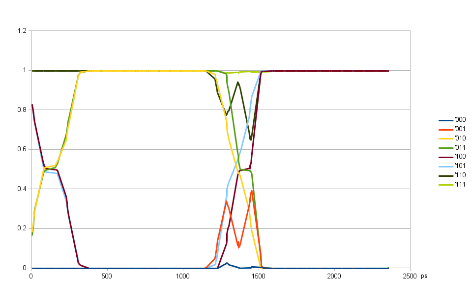
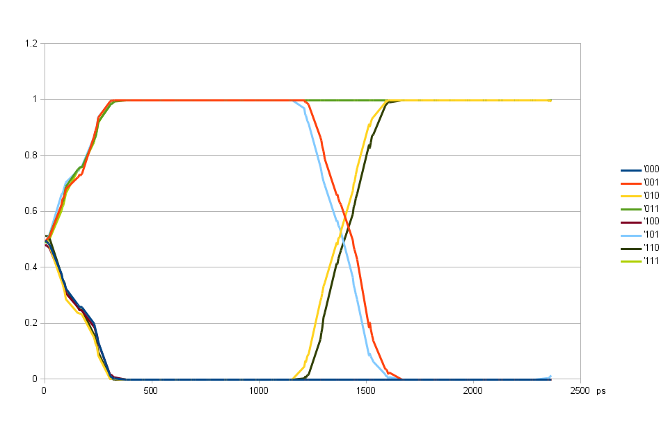
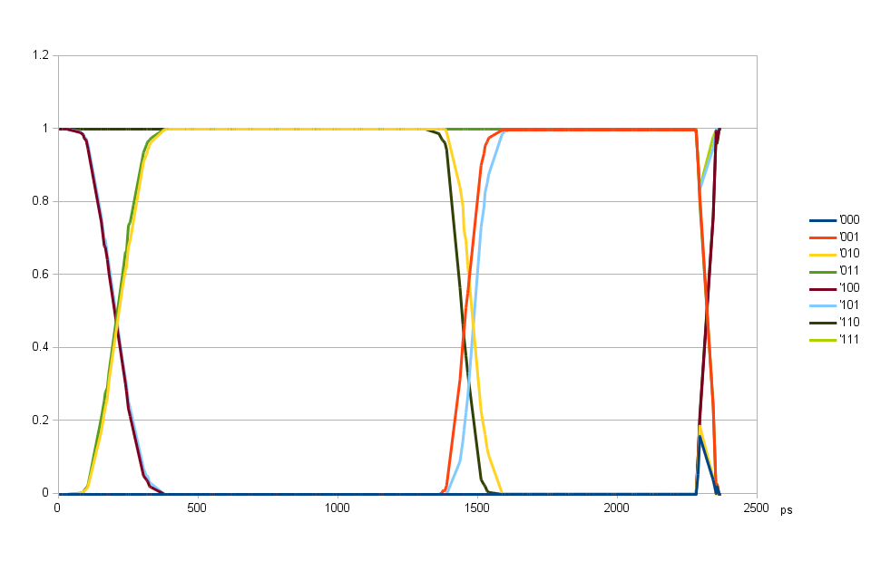
Performance measurements are implemented as a Python script (it does not look like Pythonian, most of the text was just edited from the Verilog text fixture used for simulation) running on the target system, the results were imported into Libreoffice Calc spreadsheet program to create eye diagram plots. Python script directly accesses memory-mapped AXI PS Master GP0 port to read/write data, no custom kernel space drivers were needed for this project. Both simulation test fixture and the Python script programmed delay values, controller modes and created sequence data for memory initialization, refresh, write leveling, fixed pattern reading, block write and block read operations. For eye pattern generation one of the delay values was scanned over the available range, randomly generated 512 byte block of data was written and then read back. Then the read data was compared to the one written, each of the 4096 bits in a block was assigned a group depending on the previous, current and next bit written to the same DQ signal. These groups are shown on the next plots, marked in the legend as binary strings, “001″ means that previous written bit was “0″, current one is also “0″ and the next one will be “1″. Then the read data was averaged in each block per each of 8 groups, first for each DQ individually and averaged between all of the 16 DQ signals. The delays scanned over 32 values of the main delays and 5 values of fine delays for each, the relative weight of fine delays was calculated from the measured data and used in the final plots.
Fig. 2. DQ input delay common for all bits, DQS input delay variable
DQ and DQS input delay selection by reading fixed pattern from memoryFirst I selected initial values for DQ and DQS input delays reading fixed pattern data form the memory – that mode eliminates dependence on write operation errors, but does not allow testing over the random data, each bit toggles simultaneously between zero and one. This is a special mode of DDR3 memory devices activated by control bits in the MR3 mode register, reading this pattern does not require activation or any other commands before issuing READ command.
Scanning DQS input delay with fixed DQ input delay using randomly generated dataDQ delays can scan over the full period, but DQS input delay has certain timing dependence on the pair of output clock. Fig. 2. illustrates this – the first transition centered at ~150 ps is caused by the relative input delays of DQ and DQS. Data strobe latches mostly previous bit at delays around 0 and correctly latches the current bit for delays form 400 to 1150 ps, then switches to the next bit. And at around the same delay of 1300 ps the iclk to oclk timing in ISERDESE2 is not satisfied causing errors not related to DQ to DQS timing. The wide transition at 150 ps is caused by a mismatch between individual bit delays, when those individual bits are aligned (Fig. 4) the transition is narrower.
Fig. 3. Alignment of individual DQ input delays using 90-degree shifted DQS delay
Aligning individual DQ input delay valuesFor aligning individual DQ input delays (Fig. 3) I programmed DQS 90 degrees offset from the eye center of Fig. 2, and find the delay value for each bit that provides the closest to 50% value.
Scanning takes over both main (32 steps) and fine (5 steps) delays, there are no special requirements on the relative weights of the two, no need for the combined 8-bit delay to be monotonic. This eye patter doe not have an abnormality similar to the one for DQS input delay, the result plot only depends on DQ to DQS delay, there are no additional timing requirements. The transition ranges are wide, plot averages results from all individual bits, alignment process uses individual bits data.
Fig.4. DQ input delays aligned, DQS input delay variable
Scanning over DQS input delay with DQ input delays alignedAfter finishing individual data bits (DQ) input delays alignment I measured the eye pattern for DQS input delay again. This time the eye opened more as one of the sources of errors was greatly diminished. Valid data is now from 100 ps to 1050 ps and DQS delay can be set to 575 ps in the center between the two transitions. At the same time there is more than 90 degrees phase shift of the DQS from the value when iclk to oclk delay causes errors.
Fig.4. also shows that (at ~1150 ps) there is very little difference between 010 and 110 patterns, same for 001 and 101 pair. That means that inter-symbol interference is low and the bandwidth of the read data transfer is high so the data rate can likely be significantly increased.
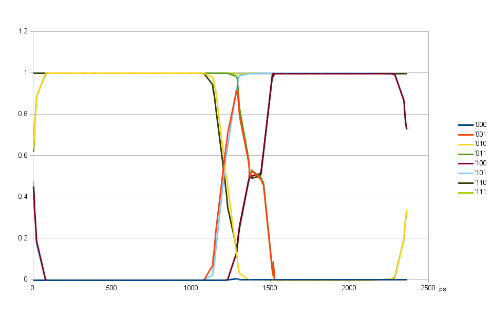
Evaluation of memory WRITE operationsWhen data is written to memory DDR3 device is expecting certain (90 degree shift) timing relation between DQS output and DQ signals. And similar to the read operation there are additional restrictions on the DQS timing itself. The read DQS timing restrictions were imposed by the ISERDESE2 modules, in the case of write the DQS timing requirements come form the memory device – DQS should be nominally aligned to the clock on the input pads of the memory device. And there is a special mode supported by DDR3 memory devices to facilitate this process – “write leveling” mode – the only mode when memory uses DQS as input (as in WRITE modes) and drives DQ as outputs (as in READ mode), with least significant bit in each byte lane signals the level of clock signal at DQS rising edge. By varying the DQS phase and reading data it is possible to find the proper delay of the DQS output, additionally the relative memory clock phase is controlled by the programmable delay in the MMCME2_ADV module.
Fig. 5. DQ output delay common for all bits, DQS output delay variable
Scanning over DQS output delay with the individual DQ output delays programmed to the same valueWith the DQ and DQS input delays determined earlier and set to the middle of the respective ranges it is possible to use random data writing to memory for evaluation of the eye patterns for WRITE mode. Fig. 5. shows the result of scanning of the DQS output delay over the full available range while all the DQ output delays were set to the same value of 1400 ps. The optimal DQS output delay value determined by write leveling was 775 ps. The plot shows the only abnormality at ~2300 ps caused by a gross violation of the write leveling timing, but this delay is far from the area of interest and results show that it is safe to program the DQS delay off by 90 degrees from the final value for the purpose of aligning DQ delays to each other.
Fig. 6. Alignment of individual DQ output delays using 90-degree shifted DQS output delay
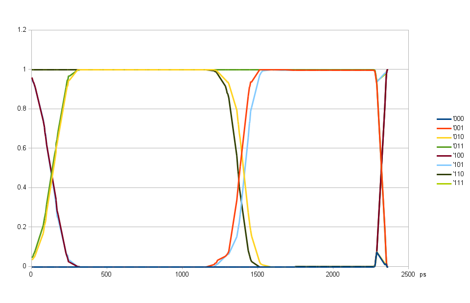
Aligning individual DQ output delay valuesThe output delay of the individual DQ signals is adjusted similarly to how it was done for the input delays. The DQS output delay was programmed with 90 degree offset to the required value (1400 ps instead of 775 ps) and each data bit output delay was set to the value that results in as close to 50% as possible. This condition is achieved around 1450 ps as shown on the Fig. 6.
50% level at low delays (<150 ps) on the plot comes from the fact that the bit “history” is followed to only 1 before the current, and the range of the Fig. 6 is not centered around the current bit, it covers the range of two bits before current, 1 bit before current and the current bit. And as two bits before current are not considered, the result is the average of approximately equal probabilities of one and zero.
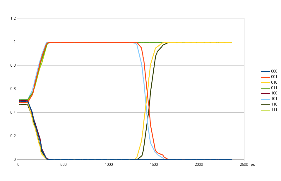
Fig.7. DQ output delays aligned, DQS output delay variable
Scanning over DQS output delays with the individual data bits alignedWhen the individual bit output delays are aligned, it is possible to re-scan the eye pattern over variable DQS output delays, the results are shown on Fig. 7. Comparing it with Fig. 5 you may see that improvement is very small, the width of the first transition is virtually the same and on the second transition (around 1500 ps) the individual curves while being “sharper” do not match each other (o10 does not match 110 and 001 does not match 101). This means that there is significant inter-symbol interference (previous bit value influences the next one). There is no split between individual curves around the first transition (~200 ps), but that is just because the history is not followed that far and the result averages both variants, causing the increased width of the individual curves transitions compared to the 1500 ps area. But we used SLEW=”SLOW” for all memory interface outputs in this setup. This it is quite adequate for the 400MHz (800Mb/s) clock rate to reduce the power consumption, but this option will not work when we will increase the clock rate in the future. Then the SLEW=”FAST” will be the only option.
Software Tools UsedThis project used various software tools for development.
- Icarus Verilog provided simulation engine. I used the latest version from the Github repository and had to make minor changes to make it work with the project
- GTKWave for viewing simulation results
- Xilinx Vivado and Xilinx ISE WebPack Edition for synthesis, place and route and other implementation tasks. To my personal opinion Xilinx ISE still provides better explanation of what it does during synthesis than newer Vivado, for example – why did it remove some of the register bits. So I was debugging code with ISE first, then later running Vivado tools for the final bitstream generation
- Micron Technology DDR3 SDRAM Verilog Model
- Eclipse IDE (4.3 Kepler) as the development environment to integrate all the other tools
- Python programming language and PyDev – Python development plugin for Eclipse
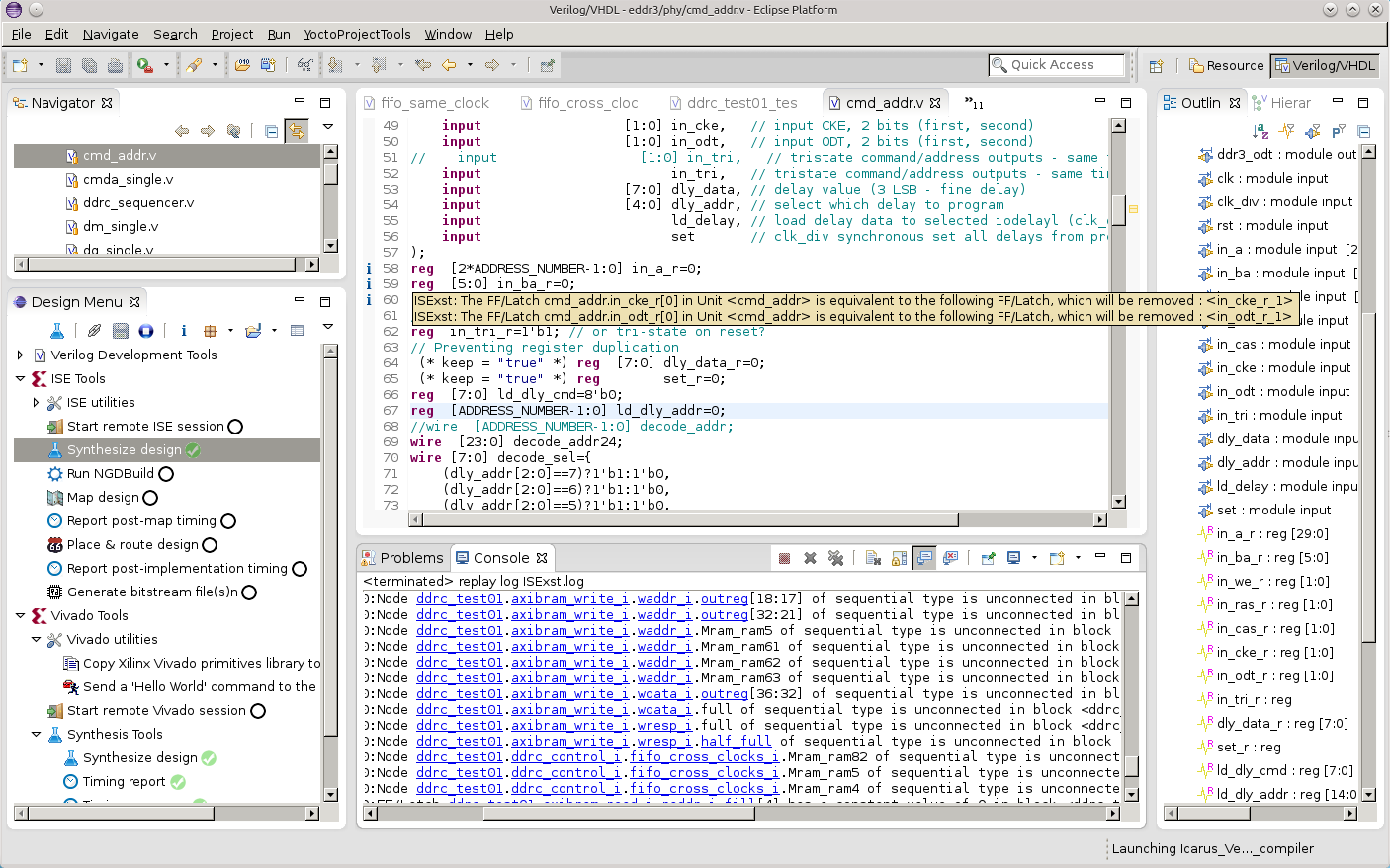
- VDT plugin for Eclipse (documentation) including the modified version of VEditor. This plugin (currently working for Verilog, tested on GNU Linux and Mac) implements support for Tool Specification Language (TSL) and enables easy integration of the 3rd party tools with support of custom message parsing. I’ll write a separate blog post about this tool, this current eddr3 project is the first one to test VDT plugin in real action.
Fig. 8. VDT plugin screenshot with eddr3 project opened
ConclusionsThe eddr3 project demonstrated performance that makes it suitable for Elphel NC393 camera system, successfully implementing DDR3 memory interface to the 512Mx16 device (Micron MT41K256M16HA-107:E) in a single HP34 bank of Xilinx XC7Z030-1FBG484C. The initial data rate equals to the maximal recommended by Xilinx for the hardware setup (using internal Vref) providing 1600MB/s data bandwidth, design uses the SLEW=”SLOW” on all control and data outputs. Evaluation of the performance suggests that it is possible to increase the data rate, probably to above the 3GB/s for the same configuration.
The design was simulated using exclusively Free Software tools without any use of encrypted or undocumented features.
Elphel, inc. on trip to Geneva, Switzerland.
University of Geneva
Monday, April 14, 2014 – 18:15 at Uni-Mail, room MR070, University of Geneva.
Elphel, Inc. is giving a conference entitled “High Performance Open Hardware for Scientific Applications”. Following the conference, you will be invited to attend a round-table discussion to debate the subject with people from Elphel and Javier Serrano from CERN.
Javier studied Physics and Electronics Engineering. He is the head of the Hardware and Timing section in CERN’s Beams Control group, and the founder of the Open Hardware Repository. Javier has co-authored the CERN Open Hardware Licence. He and his colleagues have also recently started contributing improvements to KiCad, a free software tool for the design of Printed Circuit Boards
Elphel Inc. is invited by their partner specialized in stereophotogrammetry applications – the Swiss company Foxel SA, from April 14-21 in Geneva, Switzerland.
You can enjoy a virtual tour of the Geneva University by clicking on the links herein below:
(make sure to use the latest version of Firefox or Chromium to view the demos)
Foxel’s team would be delighted to have all of Elphel’s clients and followers to participate in the conference.
A chat can also be organized in the next few days. Please contact us at Foxel SA.
If you do not have the opportunity to visit us in Geneva, the conference will be streamed live and the recording will be available.
NC393 development progress – the initial software
The software used in the previous Elphel cameras was based on the GNU/Linux distribution supported By Axis Communications for their ETRAX processors. Of course it was heavily modified, we developed new code and ported many applications to run in the camera. Over the years we worked on making it easier to install, use and update, provided customized Live GNU/Linux distributions so those with zero experience with this operating system can still use the camera development software. Originally we used Knoppix-based CD, then DVD, then switched to Kubuntu when it became available and stable. And DVDs were eventually replaced by the USB flash drives.
Knoppix and Kubuntu are for the host computer, the cameras themselves used the same non-standard, mostly home-brewed distribution, that became more and more difficult to maintain especially when Axis abandoned their processors. So even during the first attempt to move to a new platform we really hoped to be able to use modern distribution for the embedded systems. And get rid of the nightmare of porting ourselves such applications as PHP and then doing mostly the same all over again when the new revisions became available. To be able to use the latest Linux kernel and not to spend time modifying the IDE driver myself to provide support for the large block hard drives when most manufacturers abandoned 512 byte ones – 2.6.19 kernel does not have it and there is not easy to use the later drivers.
Oleg is now working on adapting the OpenEmbedded distribution and the work flow for the new camera distribution, and while embracing the power of “bitbaking” we are trying to preserve the features we implemented in the NC353 camera software. And while the OpenEmbedded-based Yocto Project is for embedded system developers, we need the software for Elphel camera users – software that can be easily installed by a single script (at least on a particular GNU/Linux distribution) or come pre-installed on a flash media. It should work “out of the box” for the users with no prior GNU/Linux experience – most of the camera users have different OS on their computers. We would also like to keep what we believe has an important practical use – a feature behind our /*source is inside*/ logo on the cameras. Each camera keeps the source code of the modifications archived in the internal flash file system, so running the downloaded from the camera script by the user results in virtually identical binary image, even if some software in the camera was custom-modified from the official (supported through Elphel git repositories) distribution.
There is still a lot left in the OE that we do not fully understand, but we are trying to do it right from the very beginning, understanding how important it is from our experience of making some major re-organizing code for the previous products. And Oleg is doing a good progress, there is a wiki page and Git repositories: meta-elphel393, meta-ezynq that document our work on this.
I did not succumb to a temptation to start working on the FPGA code immediately – there are some new ideas we want to try as well as some left for a future major “revolution” when updating the existing cameras FPGA code for the new sensors and applications. Anyway – we are not under pressure to demonstrate images from the new camera and we are confident that this job will be done in the expected time and will have the NC393 operational by the second half of the 2014. And the time is working for us – there are many people working now with Xilinx Zynq, and the active development weeds out bugs at a high rate. Failing to upgrade to the latest version already took a whole week of development time – the bug in the Xilinx Ethernet driver turned out to be already fixed.
While Oleg was immersing himself into the OpenEmbedded I was looking into the kernel driver development, what changed since the 2.6.19 era I dealt with when working on the previous camera software. There turned out to be quite a few changes and I decided to learn the new features working on a simpler drivers that we needed for the new boards. First of all I was pleased to find out that of the 7 of the I²C chips used on the 10393+10389 boards 3 were supported by the available kernel drivers – had just to specify them in the Device Tree and the supercap-powered real time clock was immediately recognized by the system – so did the temperature sensor/EEPOM and GPIO ports. Of the remaining ones with no available drivers the most challenging turned out to be SI5338 (clock generator) and I tried to add support for this device, using sysfs to control it, Device Tree (DT) to initialize it, and dynamic debug to facilitate development – none of these interfaces were used in the previous cameras.
The SI5338 had all the needed documentation available on the manufacturer’s web site, ready for download. But the device itself turned out not to be to so easy to control, and the recommended procedure included generation of the register map with the ClockBuilder software (for MS Windows), then loading the data to the device registers and initializing it with rather simple code, for which Silicon Labs provides the source. That did not seem very convenient so I tried to implement the driver that can be controlled at run time directly, calculating the particular register values from the high-level data on the fly. Most features are now supported in the si5338.c driver, it is also possible to load the register data generated by the ClockBuilder software (it is possible to run it with Wine) after converting the file with the Python script. It took me more time than I expected to develop this driver to the usable state, but I hope this work will be useful for others too. SI5338 is an excellent device that deserves better support in the Linux kernel. And having the driver working – it eliminates the last remaining obstacle to start working on the FPGA code. Or one of the last remaining – there are still a few minor ones left.
Elphel next camera – sample configuration
With all three of the new boards for the NC393 series cameras assembled (but only partially tested) it is now possible to connect them with the existent components and show some possible configurations. Main applications of Elphel cameras are scientific research, system prototyping, proofs of concepts designs – areas that routinely require unique configurations, and this new cmaer series will continue tradition of high modularity.
The camera boards look nothing like Lego blocks, but nevertheless they can zip together in different ways allowing to make new systems with minimal additional hardware. Elphel new design values our prior work (hardware development is still expensive) and provides compatibility with the existent modules, simultaneously enabling new features that were not previously possible, The most obvious example – sensor interface. The 10393 board is designed to accommodate our existent sensor front ends, custom flex cables of different lengths and shapes. That will help us to reduce the transition period to the new camera so we can focus on the high performance system board and port portions of the software and FPGA code, code that is already proven to work.
The same camera sensor ports will allow us to use multi-lane serial sensor connections needed for the modern high speed and high resolution devices, but we will work on this only after the first part will be done and we will be able to replace our current systems with the new ones. Implementation of the serial sensor connection has some challenges for us because the used protocols are not open and we have to rely only on the pieces of the available information and some reverse-engineering and research. It is not the most fun work to do, but being an Open Hardware/ Free Software company we will not provide our users with semi-open documentation. Our users will always be able to rebuild all the binaries from the source code – same binaries from the same code we have access ourselves. The only NDA Elphel ever signed was with Kodak – that sensor NDA had clear expiration time, so at the moment we planned to start distributing our products (and so the source documentation) we were not be bound by it anymore.
Sample configuration illustrated below combines the new and existent modules, the later have links to the design documentation on Elphel wiki. It is not so for the new boards (10393, 10385, 10389) – no circuit diagrams, parts lists or PCB layouts are publicly available when this post is being written. Hardware errors are usually much more expensive to fix, and we do not want somebody to duplicate our hardware “bugs” until we consider our products (“binaries”) to be good enough to go to our users. So while we set up public Git repository when we start software development, we publish our hardware documentation simultaneously with the start of the product distribution – together with “binaries”, not ahead of them.
Sample configuration of the electronic modules of Elphel NC393 camera family
- 1 – 10393 Multisensor camera system board based on Xilinx Zynq 7030 SoC.
- 2 – 10385 Power supply board
- 3 – 10389 Interface board
- 4 – Inter-board power distribution: 6-pin (3 circuits) header on the 10385, receptacles on both 10393 and 10389
- 5 – Inter-board signal connector: 40 pins (USB, SATA, GPIO)
- 6 – mSATA SSD card
- 7 – Processor heat sink (temporary). Production cameras will have custom heat spreader to transfer CPU/FPGA generated heat to the camera aluminum body or other heat sinks in multicamera systems
- 8 – Ethernet (GigE) jack, РоЕ-compatible
- 9 – DC power input (9-36V or 18-72V depending on application)
- 10 – Memory card (can be used to boot the system for cold firmware update)
- 11 – Micro USB B connector for system serial console with GPIO signals to select boot mode and generate system reset. Mounted on the 10393 system board
- 12 – Micro USB A host connector for communication with external memory and I/O devices. Mounted on the 10389 interface board.
- 13 – USB A/eSATA combo connector. eSATA port will be used for interfacing external storage devices (HDD, SSD) and downloading data from the camera internal SSD to the host computer. USB portion of the connector can provide power to the external device through the same cable as SATA data.
- 14 – 2.5mm audio type connector for external synchronization input and output (opto-isolated and directly coupled)
- 15,16,17 – directly connected sensor front ends. Compatible with the current 5MPix 10338 (shown) and other parallel data output sensors, programmable interface voltage. With the controlled impedance cables same ports will allow using up to 9 differential lanes plus I2C and 2 extra control signals.
- 18,19,20 – sensor front ends connected through 21 – 10359 multiplexer that allows simultaneous acquisition of images from up to 3 sensors into on-board SDRAM and then transferring them to the system board. In the future we will develop a faster multiplexer supporting serial links to the sensors and/or the system.
- 22 – 103695 – IMU adapter board, or other "granddaughter" extension board connected to the 10389 interface (daughter) board. Two 10-pin connectors provide 3.3V and 5.0V power, USB and 4 GPIO connected to the FPGA pads through high speed voltage level shifters
- 23 – 103696 – Serial GPS adapter board with 1pps input, uses another "granddaughter" port.
- 24,25,26 – Inter-camera synchronization (daisy chain connection) for the systems with multiple camera boards located in the same enclosure, similar to the current Elphel Eyesis4pi cameras
The setup shown above is a sort of mockup – while all the components are real, we do not yet have software to run it, even to test it. So there is no sense in powering up such a system – nothing will happen. And there is a lot to be done before we will be able even to completely test the new hardware and prepare and release revision “A” of each of the prototyped boards. We plan to be ready by the middle of 2014.
NC393 development progress – testing the hardware
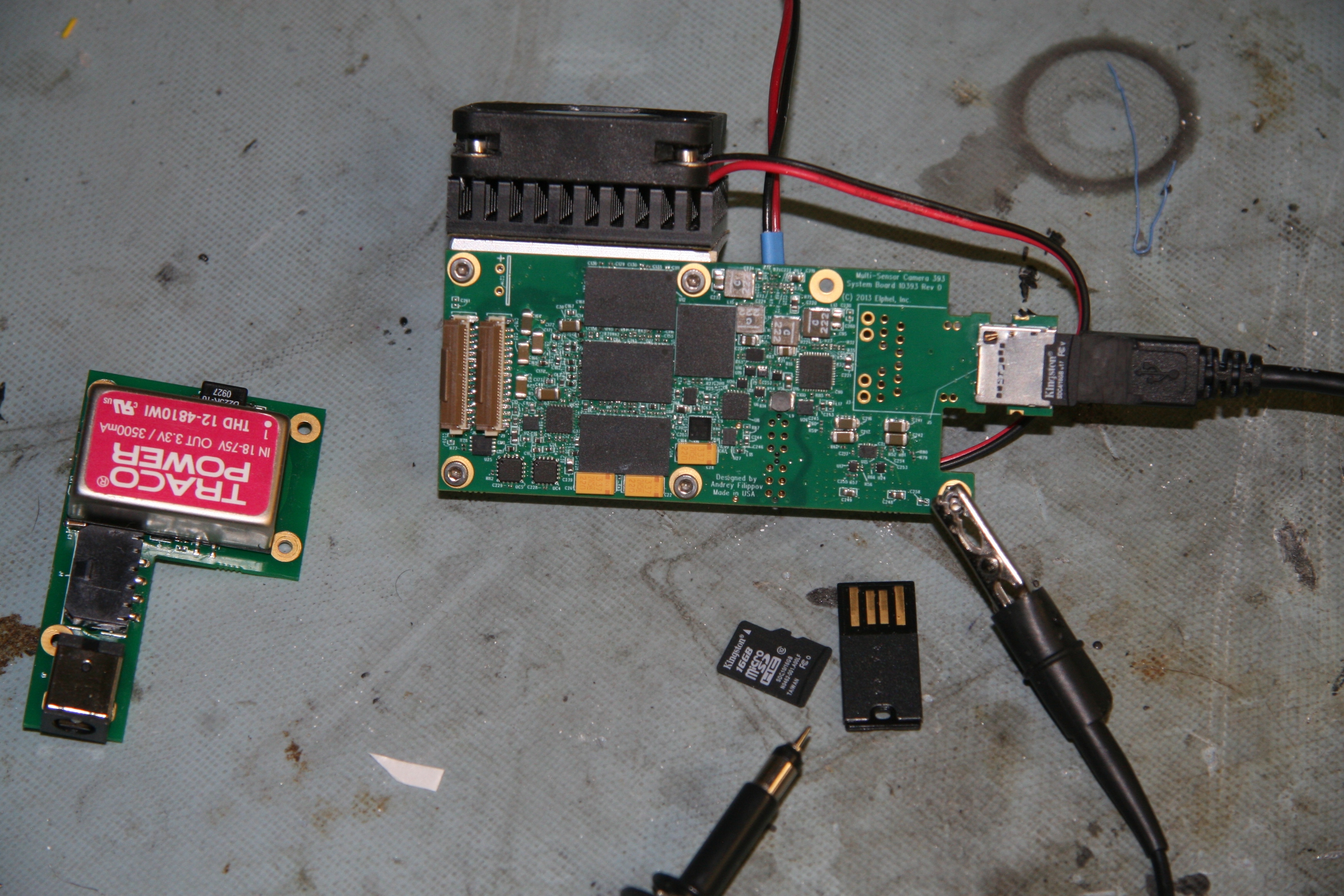
10393 board, memory side
We received the first prototype of the 10393 rev.’0″ – the new camera system board with all the BGA chips mounted. It took a little longer as our PCB assembly manufacturer had to order solder paste stencils as some chips (DC-DC converter module in LGA package and QFN chips with central thermal pads) required more than just applying tacky flux and running them through the reflow oven. The photo shows the 10393 system board together with the 10385 power supply board that I assembled earlier while waiting for the main one. This time the power supply is a separate module so we’ll not need different system board versions for different power supply options as we do with Elphel current NC353.
The shown prototype version has the full functionality, including РоЕ – feature that we will not offer in the production cameras to stay out of trouble with the patent trolls. As soon as the relevant patents will be ruled invalid we will be able to build such boards, but currently the cameras will be powered through the regular barrel-type DC jack or the 4-pin Molex connector in the multi-camera systems like Eyesis. 10385 also has a low-leakage (few microamps idle consumption) switch to use the battery-powered camera in remote locations, controlled by the system clock powered by a super-capacitor (not yet installed – there is an empty space with “+” sign on visible on the photo).
10393 with 10385 board, SoC side
I finalized the 10393 board assembly installing other components including couple hundred (bragging again) 0201 resistors and capacitors. Before starting I tested the resistance (lack of shorts) between the ground and power rails to make sure that I did not screw up pinouts during schematic/PCB design and so the board revision “0″ has a chance to be successfully tested. I repeated those tests while installing components as a power-to-ground shorts are rather difficult to locate as there are so many tiny capacitors between them.
With assembly done the board was ready for the first “smoke” test – power it up while controlling the power consumption (I used a regular test bench power supply instead of the 10385 to provide the primary 3.3V power). I was turning power on for just a few seconds controlling the secondary voltages (1.0V, 1.8V and 1.5V) with the oscilloscope. After fixing a bad soldering on the intermediate “power good” pullup resistor (secondary voltages are supposed to come up in a prescribed sequence) all 3 of these voltages were up, measured OK and the board consumed 320 mA with the system reset released but no firmware to run. There are several additional DC-DC converters on board (5V for USB and 2 independently software-regulated voltages for the external boards (sensor front ends in most applications), but these converters are turned on by the software and I did not have any at the moment.
10393 board, SoC side
Photos show the heat sink and a fan attached to aluminum angle, not directly to the Zynq chip. In production camera there will be a custom heat sink (no fan) between the 10393 and the optional 10389 interface/storage board, it will transfer processor heat to the camera aluminum body and the on-chip thermometer will be used to monitor the temperature and prevent overheating. Rather large temporary heat sink will be used during development (not to depend on the temperature monitoring software), thin angle part will allow to test the 10389 board that will nearly touch the other surface of the aluminum plate.
The next thing to test was to make the CPU (Xilinx Zynq XC7Z030-1FBG484C) run and test the DDR3 memory. If this core of the system is operational, we can test the peripherals one by one, and failures in some of them would not prevent testing of the others. If the core would fail – we’ll have to try to find out (or just guess) the problem and redesign the board, order new ones, have new stencils, assemble and try again. Of course we’ll need to re-spin the board before the production units manufacturing, but I hoped that just the next revision will be good enough to go to the users, that changes will be small. I wrote “guessed”, because if the problems would be related to the DDR3 memory operation the means to troubleshoot them would be limited – the data and address/command lines are completely buried between the chips – memory is placed directly opposite to the Zynq SoC. There are no resistor terminations on the address/command lines, the DQ lines are swapped in each byte group and the byte groups are also swapped. I relied on Xilinx documentation that they OR-ed the data lines during write leveling, so the DQ swapping will not harm this functionality.
Skipping the requirement for the address line termination allowed the overall design to be compact and the connections themselves to be really short (actually shorter than the lines inside the SoC chip itself). I used Micron documentation when considering such solution, but it still needed to be tested on the real board. Such component placement allowed me to make average length of the address/command traces 15.5mm, individual traces had to be shortened/extended to keep combined PCB delays and internal SoC pin delays the same for each address/command and for each member in the byte group for data. Internal DDR3 chip delays do not need to be considered as they are balanced inside the package. Data connections lengths (they are just peer-to-peer, no split for the two memory chips as for address/command lines) are even shorter – they average from 8.5mm to 14.5 mm for different byte groups.
Additional challenge for the initial breathing life in this new board was that we did not have the proven code to run on it, something we had for the Avnet MicroZed board while developing the free software bootloader to replace the Xilinx proprietary one. So that was a real test for our code and I decided to never even try the proprietary one on the new system.
The 10393 board has no LED (not to count 2 Ethernet jack ones, but they are controlled by the Ethernet PHY), so I temporary borrowed one GPIO signal from the MDIO bus (Ethernet PHY control) to be able to step through the boot process not relying on the serial console to be operational. I just put the LED there without any transistor, so the 1.8V-powered diode was really dim, but that was OK. And the serial output turned out to be alive immediately so there was no real need for that debug tool and I was able to remove those extra wires. The board got to U-Boot prompt immediately, but unfortunately – not every time. So I had to spend several days (one of them because of just the faulty micro-SD card that silently replaced one sector with garbage even when read back by the computer) figuring out the instability. I still do not understand exactly what is wrong (it happens when the relocated code switches the memory mapping and copies itself back to the low addresses), but just adding delay by copying that range twice resolved the issue, it turned out to be software-related one as it was present when running other (proven) boards also, not just with the 10393.
The core of the system is now verified, automatic write leveling and the two other hardware-implemented memory training functions produce reasonable results and the delay settings seem to be rather forgiving. That confirms the PCB design and makes it possible to move forward with testing of the other peripherals and starting the FPGA part of the design.
There are other urgent projects at Elphel I have to be involved now, so not yet working on the NC393 full time, but this makes really good news for us to pass the important test. Booting the new board with just the free software, no proprietary tools at all – it is also very encouraging. Xilinx just released the new version of the tools, the human-readable (html) part of the FSBL output looks even fancier than that of Ezynq, but I believe ours is still more convenient to work with – we made it for ourselves, and so for other developers (who are like us) too.
Flight-machine
This page gives brief overview of multirotor UAV platform called “Tau”, which is built specially for participating in flying robots contest which is established by Croc company. Our team name was “Autonomous aerospace”.
Doing contest machine we were not looking for easiest way of implementation. Some of the purposes are:further developing of our autopilot and getting experience of integrating machine vision functionality in real-time into control loop.
During contest preparation we dealed for a first time with multyrotor platform . There was only airplanes autopiloting experience before. Adopting autopilot for quadrotor was not so obvious as we expected, but we succeded. Now proudly can say, that we built first quadrotor which calculates all the navigation and control math under QNX real-time operating system . At least no one did any crazy stuff like this before
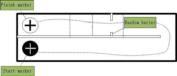
MissionMission is to take off from start marker, follow simple maze toward finish marker, touch down within its contour and than fly back. Then landing on start marker and cutoff engines. On path to target random barrier is set. It can be moved by organizators across the wall and gate might be aligned at left, at right or anywhere between walls.
Drone is allowed to touch walls, but not allowed to touch the ground.
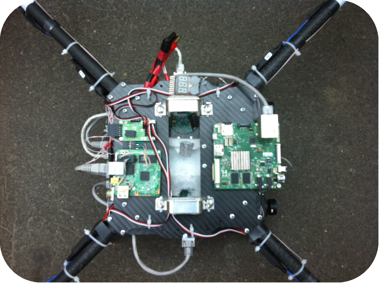
On-board UAV control system Computers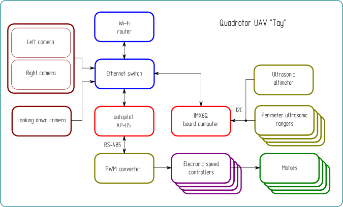
Central control unit is autopilot AP-05 (AP). It has embedded inertial navigational system (INS), air data system (ADS), global navigational satellite systems GLONASS/GPS (GNSS). Computer in AP-05 – is ARM9 family processor with 400MHz clock frequency and 64 megabytes of RAM. Operation of computer is conducted under QNX Neutrino real time operating system (RTOS) control. QNX is used under academic licence. Major point is implementation of navigational and control loop under QNX by separate processes: fnav for navigation, fcont for control. Loop frequency is 200 Hz.
Decicions for flight in contest maze is made in autopilot by setting input values for roll, pitch and yaw PID regulators.
Machine vision computer (MVC) is i.MX6Q SABRE lite board with 4 processors of Cortex-A9 archetecture. For the research of QNX technologies machine vision is also computed under QNX.
Connection between AP and MVC is made by Ethernet via native qnet protocol.
For the programmer is gives transparency and flexibility, all interprocess communication is unix-like locally or remotely by qnx messages. Local is conducted by kernel, remote by kernel+qnet.
Sensors
As a proximity sensors ultrasonic rangefinders SRF08 are used. They are mounded at bumper each for front, rear, left, right sides accordingly. Same sensor is used for altimetry. Sensors are connected to i.MX6Q SABRE lite (MVC) via I2C interface to the same bus with different adresses. Doing altitude and wall navigation control loop over such a long way looks weird. All because AP doesn’t have external I2C due to its noise vulnerability. Process which polls range finders reflects data to the system by /dev/fsrf resource manager. Autopilot reads this data over qnet stack like /net/mvc/dev/fsrf file. After reading by navigational process range data is filtered and after reflected as feedback for altitude control and wall avoidance algorithm.
When we were looking for camera main problem was making an software interface for OpenCV in QNX. Making port of webcam USB interface to QNX in a short time seemed impossible, because of lack of knowledge in that field.
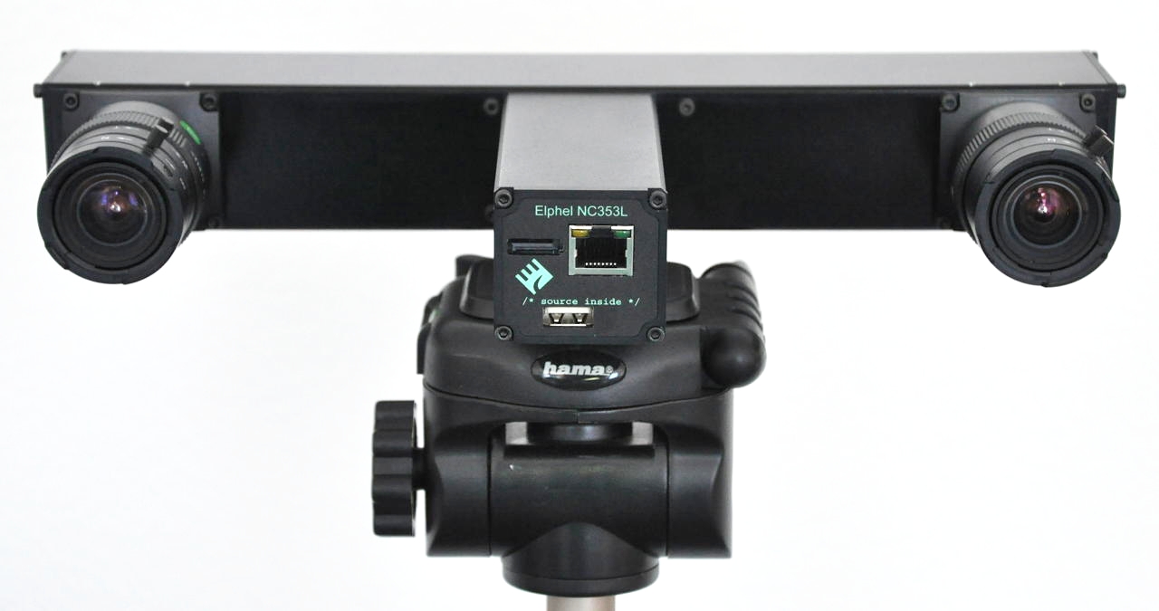
Thats why search for camera was narrowed only on IP cameras. Finally Elphel NC353L was found. It has several software interfaces for image: MJPEG over RSTP; HTTP. Camera has opened sources, so it seemed guaranteed way to make own low level protocol and image pre-processing.
Also camera has multiply configurational parameters for optimizing real time picture. Additionally matrix has higher resolution, than other cameras in same price segment.
With understanding that camera is open sourced we estimated our chances to miss appropriate solution as very low and this estimation was correct =).
Calculation of machine vision algorithm is conducted by process called fmv, and its discrete results is represented at /dev/fmv resource manager.
Machine vision
Start finish markers search
Searching for start/finish points is done by comparison of current image colour histograms with histograms of reference images. Histograms for B,R,G channels was compated accordingly, and then integral weighted estimation of similarity was calculated. Similarity is calculated separately for start and finish markers.
Stereo vision
For the barrier gate entrance we initially decided to implement stereo vision algorithms to determine its position. At the beginning of contest preparations width between walls on final approach to finish marker supposed to be 20 meters. It seemed challenging to find gate with 3m width. Thats why we decided to integrate Elphel NC353L solution. This version has multiplexor board, which simultaniously gather both sensor data to single image. Stereo camera was generously provided us by Elphel company to participate in contest.
We had previously tested semi-global block matching algorithm (SGBM). Method gives disparity map from two images. Using SGBM method, requiers distortion remap and aligning preprocessing of input images. Using matrices of internal parameters of cameras we performed images rectification, so left image row coincides with rows of right image. Experimentally we tuned scene parameters and looked for optimal diversity map. Diversity map has same dimentions as input images, but consist of 16 bit depth values. Seeing on single row in the middle of image, selected by INS to fit horizon we recoverd distance to near objects and supposed to determine gate.
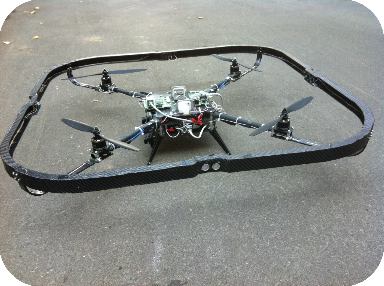
Multicopter UAV Tau frame design
Starting from the design…
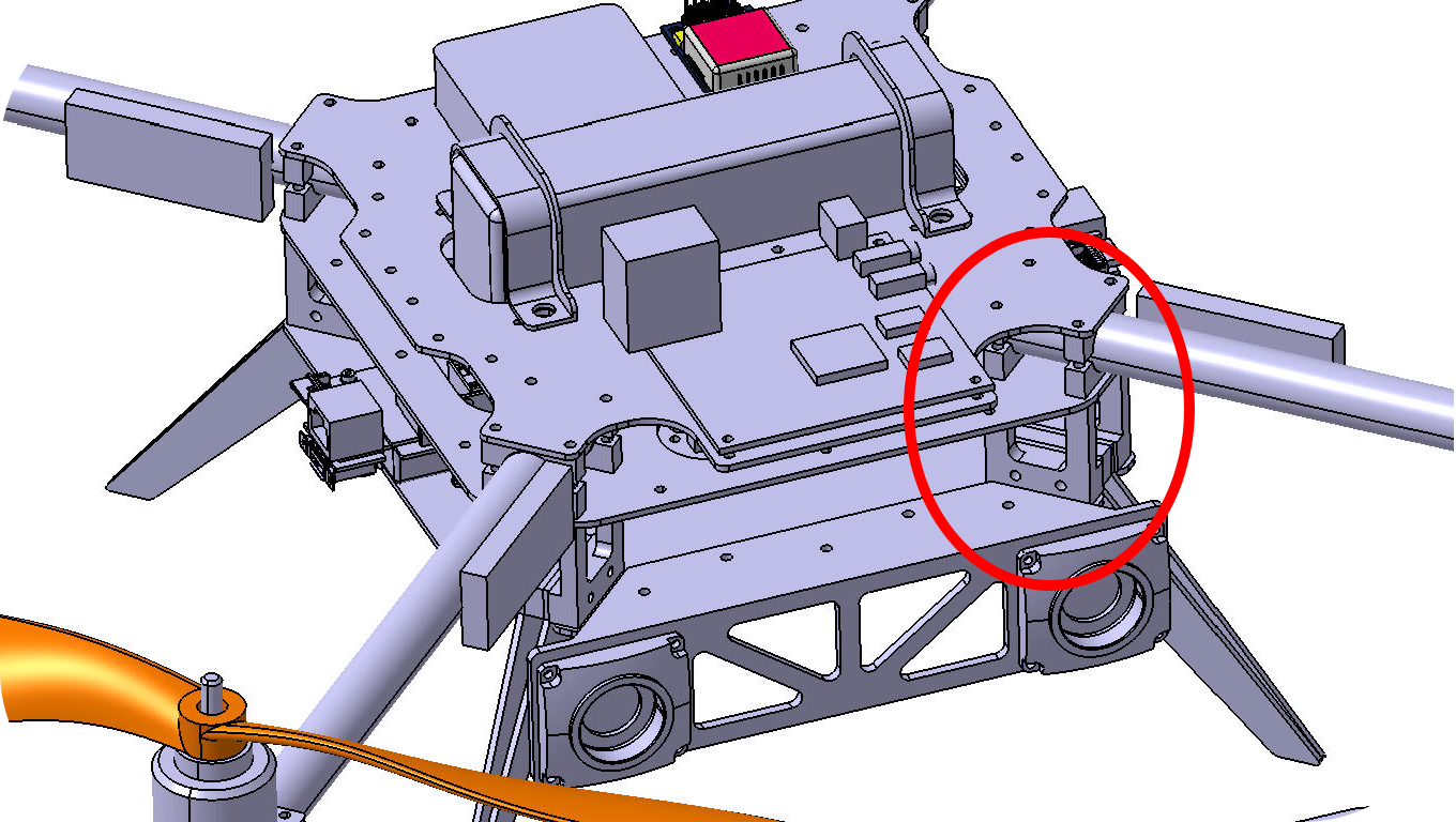
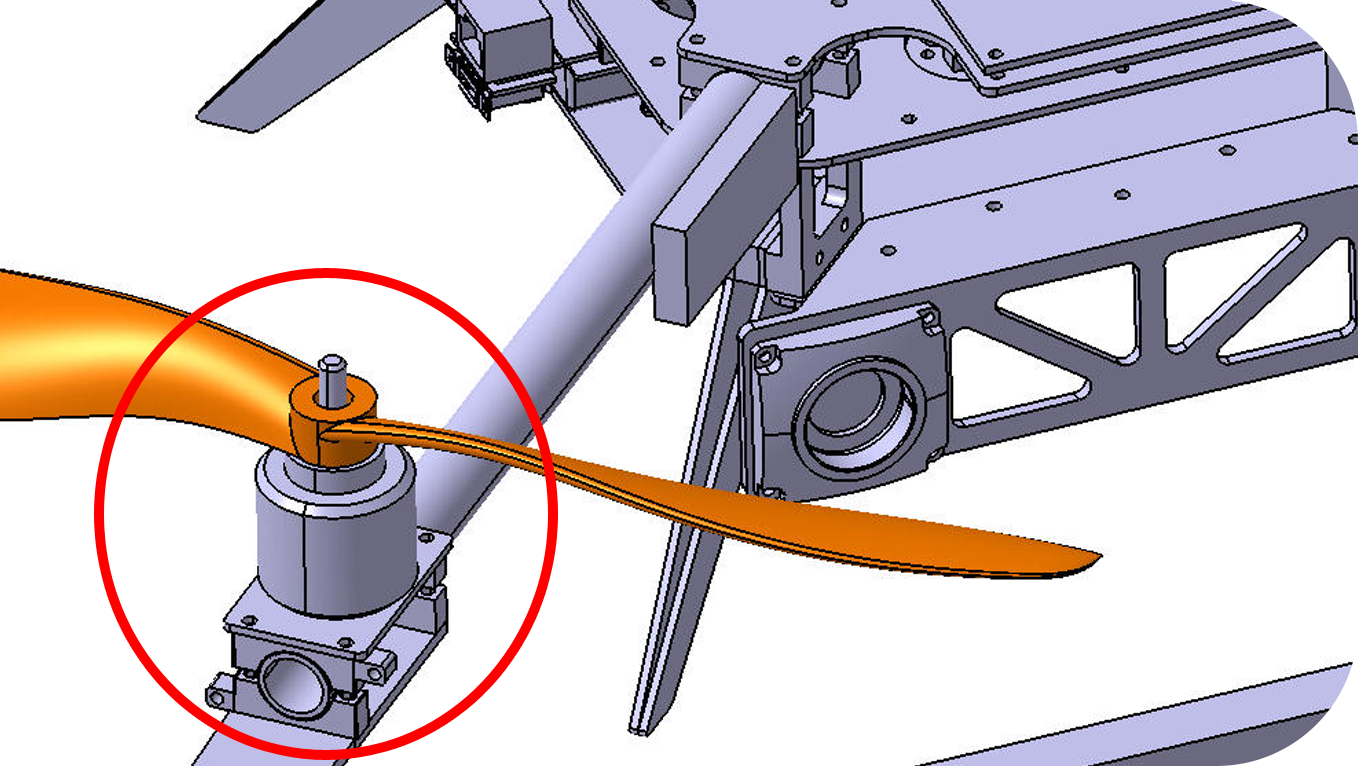
For compact setting of all required devices we decided to make central frame with 3 levels. Each level is milled carbon fiber plate. Level plates are fitted together by aluminium spacers. Between first and second levels there are carbon beams that are tighten between aluminium clamps. At the end of each beam motor is mounted using aluminium brackets. Motors are working with 12″ x 4.5 propellers. For the protection of propellers and equipment special bumper was made. 4 parts form closed perimeter. Bumper part has U-like cut and made of carbon 3 layer composite sandwich. Mounding of bumper is made by Г-like bracket, which is fixed at bottom of motor mount. After design process production and assembly started. Fristly carbon fiber plates and beams were baked. Parallely all aluminium parts were milled. On preparated plates we milled them on CNC. Then molds for bumper and brackets were milled.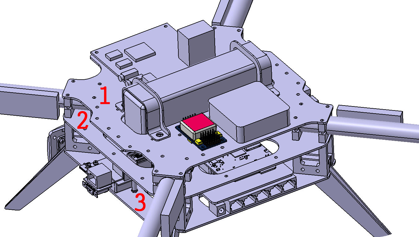
After all assembly started!
In a five days we fit everything together and made wiring of all devices.
Design of airframe in STEP format is freely avaiable: with all equipment and as plain frame.
Flight testing
When everything were done on assembly 10 days before contest begin left. Actually we had flight test platform before, so we started not from scratch in a flight software.
Previous results were got on fiber glass strong frame before. Some explanations are made on russian in following videos:
After contest drone assembly we spend 5 days to make it flight properly: maintain attitude and regulate distance from the walls.
Next five days we spent to test all mission algorithm in a combination with machine vision and real markers. We’ve got some sucessful complete tests, but all system was very unstable. Most of the problems was about flying. A lot of time was eaten by i2c rangers problems: high current of motors and vibration were making contact and ground potential unstable, and it lead to bus stuck. When bus stuck, altimeter is also stucks, what was leading to engines turn off. Many thanks for our designers and all mechanical shop. In dozens of fallings we’ve once broke bumper braket, and one leg.
Algorithm for maze flying is classical, keep right, keep distance from the walls and pray . We do not making turns, UAV maintains yaw, which is set on initial alignment. And it is aligned by rear side toward right direction at start. So it begins to fly backwards, than left, then front. And on a flight back – in reverse.
Fly front means to hold distance from front wall. When wall is far, front ranger is saturated in its maximum value, so regulator moves drone forward, by tilting its pitch front.
Contest video
In a real contest (sizes were officially corrected) distance between final approach walls became 5 meters, so finding gate was not a such big problem anymore. So barier detection was made in autopilot by finite state machine. If front stereo camera (by one of its eye) have seen ellipse in front of it, that means we have passed the gate and must see marker soon by looking down camers. If no, we probably holding right now distance from the barrier wall and must move left.
First attemptIt was failed because of improper finite state machine criterion for barrier avoidance. Drone thought that it has reached barier and next cycle it thought it has reached front wall at marker, didn’t find any markers and turned back.
Second attempt
Here we have our machine vision algorithm failed. Camera didn’t recognized landing marker, so drone tryed to find on the way back and it was dead end of algorithm.
As always there were just a question of two days of debugging to make everything right
Conclusion
We have not completely succeeded, but we have not failed.
Our team dramatically improved existed software and developed new direction – machine vision.
That was great teamwork experience, that charged our team to handle further challenges.
FPGA is for Freedom
In this post I write about our current development, my first experience with Xilinx Zynq, and also try to summarize the 10+ years experience with Xilinx FPGA devices. It is a mixture of the admiration for their state of the art silicon devices and frustration caused by the software. Please excuse my sometimes harsh words and analogies – I really would like to see Xilinx prosper and acquire software vision that matches the freedom that Ross Freeman brought to developers of the electronic devices when he invented FPGA and started Xilinx.
We planned to update our current line of cameras for some time – Elphel current model NC353 is in production for almost 7 years. Thanks to the Xilinx FPGA, it is possible to upgrade it long after it was built. In 2009 we developed the new system board, built a first unit and started working with it. This board was designed around new (in 2009) Xilinx Spartan 6 and Texas Instruments DaVinci processor. Memory and the CPU performance were increased, the board could support two sensors simultaneously (instead of just one in the older models), but in the 10373 camera system board I was not satisfied with the bandwidth of the datapath between the FPGA and the processor – it was enough for current sensors but in my opinion it did not have enough margin for the future sensor upgrades and we decided to put this project on hold and look for the better match between the CPU and FPGA.
Later we heard the news about the coming Xilinx Zynq devices, but initial rumors indicated that it is very unlikely these chips will be supported by freeware development software. Luckily, that proved to be wrong and Xilinx announced that most of the devices (excluding only the largest XC7Z045) will be supported by the free for download WebPack. Zynq combines dual core ARM CPU (with a rich set of standard peripherals) and high performance FPGA on the same chip, so it should be an exact match for our purposes and intrinsically high bandwidth between CPU and FPGA – parameter that killed our NC373 camera before it was born.
Impressed by Zynq when working on the board designThe news was really exciting, and I was waiting impatiently for the new devices to become available and the free for download status of the required software to be confirmed – many of Elphel customers are developers and we can not force them to acquire software that would be more expensive than the hardware they purchase from us. By June 2013, when I was able to designate time for the full time work on the new project, both conditions were met and I started working on the circuit and PCB design. Zynq features looked very nice and documentation was quite sufficient to work on the design, it turned out to have some little but very convenient bonuses like decoupling capacitors embedded in the package – we use memory mounted on the opposite to the CPU side of the board so it is difficult to have short decoupling connections for both of them. High speed serializer/deserializer capability of virtually all of the I/O pins made it possible to have the dual-function sensor port connectors compatible with our current sensor front ends (SFE) with 12-16 bit parallel interface and capable of running serial links (such as multi-lane MIPI). Backward compatibility will reduce time before we’ll be able to start shipping NC393 cameras (and replace system boards in our Eyesis line of products), high-speed serial capability will allow cameras to keep up with new emerging high-performance sensors.
Initially, I planned to have only 3 sensor ports: one GTX to implement SATA interface, some GPIOs for inter-camera synchronization and interfacing daughter-boards (similar to what we had on our 10369 interface board for the NC353 camera) and dedicated DDR3 memory. Yes, Zynq has really nice access from the PL (programmable logic – FPGA part of the chip) to the system memory, but it is still beneficial to have memory that is not shared with the CPU and has a specialized controller fine-tuned for image processing applications. And I thought I’d need 676-ball package to fit all external devices. But by carefully going through the documentation, I realized that with the flexible I/O banking of Zynq it is possible to fit everything needed in a significantly smaller 484-ball package and to have four (instead of just three) sensor ports.
A small cloud on the horizonWhen working on the circuit design, I needed to make sure that the pins I designate for the DDR3 memory interface are valid – such interface implementation is rather challenging and there are multiple rules that have to be satisfied simultaneously. Even as we do not plan to use Xilinx stock memory controller in the camera, I thought that the software “wizard” that instantiates it in the design may be a good tool to verify the selected pinout – that’s all that I needed at this stage of the design. So I went ahead to install the software. During this process, I learned that to use freeware software (and I already explained why it is the only kind of the non-free software we can use for our products), I have to install mandatory component that transmits data from my computer to Xilinx. It is funny – being a free software/open hardware company, we post all our development files on Sourceforge, but they still prefer to dig in our “dirty laundry”. This was very unpleasant news, and the license agreement stated that, because of the nature of the Internet, they have no responsibility if any of the information they get from my computer will accidentally get to where it was not supposed to get to. OK, I decided, I’ll deal with it later when I’ll really need it to work on the FPGA design; for now, I just need to install it and try the memory controller generator, then after; uninstall the software (hopefully together with the spy agent).
Unfortunately, as it often happens, the “wizard” turned out not to be smart enough, and it told me that the 16-bit wide DDR3 interface I needed will not fit. I did verify the rules stated in the documentation again, searched online information on questions and answers about similar cases – all confirmed that the capable Zynq silicon could handle the job, but the software “wizard” prohibited it. It is quite understandable that software programs have their limitations, but when the software pretending to be “smart” is inflexible, when it (as most of the non-free code) does not allow user to comment out (to disable/bypass) specific checks, it causes frustration. So this software tried to make Zynq look less capable than it actually is, and also tried to convince me that instead of the 484-ball package, I should use larger 676-ball one, leaving less room for other components. Larger package would be more expensive for our customers too, of course.
So I just decided to move on with the circuit/PCB design regardless of my disagreement with the software – this development was described in the several previous blog posts.
By the early August, the PCB design of the Zynq-based camera system board (together with the two companion boards) was finished. I went through all the design again trying to weed out as many design errors as I could, and later that month we released the files into production. While waiting for all the components to come and the PCB to be manufactured, I started to look at the first steps in the software development I will need to be able to verify the board design. I was expecting to take the U-boot files developed for existent Zynq-based evaluation boards and tweak them to match our hardware – a rather straightforward process I did before when breathing in life in other systems. So first make U-boot work, then – proceed with the Linux kernel – both “Linux” and “U-boot” were mentioned in the documentation so I was sure I understand the overall process. I was wrong.
FSBL – a piece of proprietary code generated by the proprietary toolsOf course I understand that it may take another ten years before Xilinx will realize that the combination of the “blank tape” idea of the FPGA that they pioneered with the “totalitarian” style of development tools software is not very efficient – I’ll get to this topic later in the post. At the moment I was just looking for the Open Embedded – based distribution for existent boards that I can modify for our hardware. Internet search revealed that I still have to use proprietary tools to generate the first stage boot loader (FSBL) – piece of code responsible for the hardware initialization. This code is launched by the RBL – embedded in the chip ROM boot loader and in its turn the FSBL (starting from the Zynq OCM – internal on-chip memory) initializes external DRAM, loads and launches U-boot. Then it is the U-boot’s responsibility to take it from there and load and pass control to GNU/Linux (in the sequence that interests us). Starting with U-boot, all the code is Free Software (under mandatory for this software GNU GPL license), but not the FSBL. OK, I thought – I’ll use the tools to generate a binary blob and we’ll distribute it with our cameras. Elphel users will be able to use just the free software to re-build the camera flash image as they want. Binary blobs are nasty, and Richard Stallman would likely refuse to deal with our cameras, but we are living in the real world and so need something to start with – we can try to replace that piece of code later.
What I was not sure about was the legal status of such distribution, at least all the text files generated had Xilinx copyright and “all rights reserved” notices in the header. Funny thing is that they also have “this file is automatically generated” in the same header. To me “generated” sounds more like “created” than “copied” or “compiled” and I did not know that robots are already recognized as authors of the original works covered by the Copyright Law. So I asked this question on Xilinx forum but I was not able to get a clear answer to that question – can we redistribute FSBL custom-generated by Xilinx tools for our hardware?
We did try to generate FSBL with the tools – I failed to install the software on my computer – probably because it had too old of a version of Kubuntu and there was a conflict between the libc6 on my system and the licensing software (this funny make-pretend licensing of freebies). Oleg was luckier than me – he has a current Kubuntu version, but his operating system was still not perfect and did not completely match the development tools. When he tried to re-assign MIO pins in the tools GUI – nothing seemed to happen. Later he discovered that it actually did change; it just did not show the changes. So when he pressed “Save” and opened the same page again, there were the new (modified) values there. A little trick, but it made possible to proceed with the tools.
There are other things that I did not like in the recommended way of the FSBL generation. One is that though I usually prefer a nice GUI to the “black screen” of the command line interface, there are some definite limitations. I like GUI when it saves me from remembering a lot of commands and command options – it could be OK if I had to do my job in a relatively small area. But in a small company, we have to often switch from mechanical design to web development, Verilog code debugging, kernel drivers or image processing – all these activities have their specific tools. But GUI for new board configuration is not that useful according to my personal experience. A standard configuration file with many properly commented settings is more convenient. Configuring a new Zynq-based board for most developers is something they do not need to perform a dozen times a day – once a year is a more reasonable estimate. When you develop a new board you have to go through many manual steps: studying documentation, looking for the board components, and developing a circuit diagram and PCB layout. Going through a long list of settings, reading comments and optionally modifying some values is a very useful process for the new board, as it can help to avoid design errors that would be left unnoticed if you just clicked on several GUI buttons. Adding more configuration parameters to GUI is usually more expensive than just defining more configuration values, so more parameters are likely to be hard-coded in the software and so out of user control. Another problem of the GUI approach – I was concerned I would eventually hit a similar problem I already hit with the smart Memory Interface Generator I described above, the problem that was always a nightmare for me when I had to upgrade the FPGA development tools – new version often refused to compile the code that worked with the old version, changed the rules that are impossible to bypass. And as the code is closed, you do not have many options to tell the software that you are the boss, not it.
Configuring Zynq hardware for a commercial evaluation board with GUI – it may look cool, but the configuration is mostly already defined by the board design, so each board can come with the board-specific long and boring (but nicely commented) configuration file.
The Ezynq projectConsidering all these shortcomings of the use of the FSBL I decided to evaluate feasibility of bypassing this proprietary code completely. According to Xilinx documentation, it seemed possible, and we did not need all of the functionality of the FSBL and the FSBL generation software. We definitely do not need booting of the secret code (Zynq has elaborate hardware and software support for such feature); we also do not need to configure the FPGA portion (PL) until the system is running operating system (FSBL allows early configuration). Our plan was to add extra functionality (previously handled by FSBL) to U-boot itself so all the board configuration is done with #define CONFIG_* statements in the appropriate header files. To prevent conflict between the new parameters and already existent Zynq-related ones in U-boot name scope, we added ‘E’, starting all the parameters with “CONFIG_EZYNQ_” – this is where the project name came from. The project is available in Elphel Git repository at Sourceforge.
For this unexpected project, we purchased a nice small MicroZed evaluation board (it is the first evaluation board I ever used in my career) so we had an official software that boots and runs on this board. Even implementation of the subset of the FSBL functionality, with configuration files ready for only one board, having several known (and probably plenty of unknown) bugs, took me a whole month of programming. In that process I had to go through the documentation on many of the Zynq peripherals and their control registers, DDR3 memory interface – that will likely help me when developing the software for the actual camera. While working on the reimplementation, I was comparing the generated FSBL output against documetation and noticed several mismatches between the two, but none seem to be critical. Our code will need some cleanup – at the beginning I did not know the exact details of what will be needed, and this is my first program in Python, but the program proved to work and we’ll maintain it and use it with future Elphel camera software distributions. I also believe that there are other developers who share my view that the best FPGA silicon on the planet deserves different software, software made for the developers – not just for the cool looking presentations. And we would like other developers to try this code, creating configuration files for the Zynq-based boards they have. There are more technical details in the README file in the git repository and we are always willing to answer questions about this program.
Why I believe Xilinx will turn towards Free SoftwareWhen Ross Freeman, FPGA inventor and one of the Xilinx founders, compared the new device with a “blank tape,” he defined the future of the new class of the devices; devices where the user, and not the chip manufacturer, is in full control. It would be like it was with the magnetic tapes where people could record whatever they liked, and not just what the record companies did. It was especially important in the USSR, where I was born – the most famous and loved by the Soviet people Russian singer, Vladimir Vysotsky, “lived” mostly on the magnetic tapes recorded by people against the will of the Soviet government. Magnetic tapes were the medium that brought us the Beatles – we loved them and perceived them as a “Band of Freedom.”
Freedom is the intrinsic feature of the FPGA. I think it is better than “Field” for the first letter in the acronym. Unfortunately, the analogy with the “blank tape” does not go much farther – in the non-free country, we were free to use any brand of the tape recorder (domestic or brought from abroad) with the same tape. If the Soviet government had the same level of control over the recorders as the FPGA manufacturers have now over the required development tools, we would never be able to listen to Vysotsky or the Beatles.
Some ten years ago, Wim Roelandts, then CEO of Xilinx, had a presentation in Salt Lake City that I attended. When answering questions, he said that more than 98 percent of the company revenue comes from the FPGA (“blank tape”) sales, and less than two percent from the software. Maybe the numbers have changed by now, but I do not think the difference is radical.
I can only guess at what the rationale behind the idea of reducing the value of the main (98 percent) product for the questionable benefit of a two percent byproduct is. They probably can not believe that freedom may be monetized, it increases the value (and the lack of it – decreases) of the underlying product by more than those tiny two percent. They may think that it is irrelevant, and as they produce the best tape in the world, they should use it to the competitive advantage of their tape recorders.
There is the other side of this. Totalitarianism is not competitive in the long run. The USSR was strong in the middle of the 20th century and was able to win against Hitler in WWII. Just 10 years before its collapse, I could not believe that any change would happen in my lifetime – but there is no more USSR now. In the end of the last century (and the beginning of this one), Microsoft was considered the most successful software company, a model for others. And I see some similarity between the two – trying to keep everybody under control – be it with the help of the KGB or EULA. Soviet people did not have private property (only so called “personal property”) – virtually everything belonged to the State. Same with the users of proprietary software – you do not own what you paid money for, you are just granted a temporary right to use it. Microsoft is far from over, of course, but it has seen better times, and few are considering it as a powerful Empire now. Yes, they still dominate on the desktops, but the same approach failed in the modern areas of the web and mobile devices. In these days you have to give more control to the users – or risk becoming irrelevant. Initially Apple tried hard to prevent “jail-breaking” and not to let people to install their own software. Yes, they sure still have a lot of control, but even they had to yield some of it under the pressure of the users and competitors. It is even more valid for the faster growing Linux-based Android devices.
Xilinx itself is gradually migrating towards Free Software, at least for the code that runs on their devices. I believe this process is welcomed by Xilinx developers (who made a great job in coding Free software submitted to at least Linux kernel and U-boot) but is still not embraced completely by the management who (software-wise) got stuck in the 20th century, when the microsoviet type of the program was a model to follow. But this fight is an uphill battle, and they have to “surrender” more and more. Xilinx SDK is already based on Free Software Eclipse IDE and software components licensed under GNU GPL. I count on this trend and think that it will provide Xilinx with their own experience and prove to them that developing Free Software gives more value in return by expanding application areas and results in increased market share for the devices.
But this shift to Free Software does not yet apply to the main part of the software tools – tools for the FPGA or programmable logic (PL) in terms of Zynq development.
The Xilinx proprietary stronghold that still seems as stable as the USSR in early 1980-s is the FPGA development tools. They do not see much pressure to stop effectively crippling their hardware by the software because 1) Xilinx FPGAs are still the best and 2) Xilinx competitors cripple their products no less than Xilinx does itself. When I first started using reconfigurable FPGA in 2002, I was considering Altera too, but even their freebie software license had to be renewed each 3 months, so there was no guarantee that you’ll always be able to use the code you previously developed.
Competition on the FPGA market is increasing, and in addition to the traditional Xilinx+Altera duopoly, new players are emerging, such as Achronics and Tabula. It seems to me, however, that their bet to beat duopoly is based on the sheer technological advantage of the Intel 14nm process, not on the developer-friendly software that can really make a difference in this field.
Installation of the “spyware” as a mandatory component of the freeware FPGA development tools (in the paid-for versions this functionality may be disabled, but it is on by default) seems to be considered of high value – otherwise they would not risk alienating their loyal customers. Why do they do it? Probably in a desperate move to get more of the real life examples to improve their place and route and other related algorithms. I am not a specialist in these algorithms, but generally they are NP-hard and there are many approaches how to find good-enough solutions and improve them. And this involuntary feedback through the spyware is needed to train the algorithms being developed. Translated to USSR analogy, it would be as utopian as to assign 3 KGB agents to every citizen to find out what each of them wants and then decide in some centralized way how to make them all feel happy. Or Apple watching on the customer use of the phones to guess what they need and designing all the apps in-house that are currently available from the independent developers. Proprietary operating systems closed to developers and fully controlled by a single company already proved their inferiority on the mobile devices where they faced a real competition.
Xilinx has a unique opportunity to change this unfortunate state. They develop, produce and sell the Real Things, and Xilinx can become as recognized in FPGA development software, as it is recognized for the FPGA devices now. They are in a position not just to invest heavily in the Free Software infrastructure as IBM and other companies do, but to do much more: jump-start and lead the new class of the FPGA development tools – tools where users are partners, not just the subjects of the surveillance. Starting and maintaining a framework of the Free (not freeware, like WebPack) tools could make a real difference and create value, like independently designed apps create value for Apple or Android gadgets. Just look around – it is the second decade of the 21st century, not the late 20th. Let users (and Xilinx users are really smart developers) get to the controls – they will innovate, and some may find solutions that would never come to the mind of Xilinx staff engineers.
One may say that Xilinx already has an App Store equivalent, but the marketplace for IP cores (“vinyl records” that can be copied to the “magnetic tapes” under certain conditions) is not a substitute for the free and open FPGA development framework – users can exchange (under various free and non-free licenses, with or without compensation) their “tape records” themselves without any Xilinx involvement. In our current design, we too plan to use at least one Verilog module designed by others under GNU GPL license, and we will handle it between us and the developer directly. The other difference is that iPhone users are just phone users and the apps they download increase the functionality (and, in effect, the value) of the phone they purchase. When an FPGA developer uses a core designed by others – she just gets part of her job already done. But the increased functionality of the tools is still needed, and this functionality is usually related to much more elaborate activity than that of the casual phone app user, and FPGA developer is more likely to be able to contribute back. That does not mean, of course, that many developers will contribute new P/R algorithms, but evaluating different algorithms (including experimental ones), tweaking parameters of the goal functions – especially when the default setup can’t make it for the user - this is what many (myself included) can do. It is especially likely to happen if the users are provided with some meaningful comments on the nature of the algorithms and variable parameters.
Such development framework will make it possible for independent researchers to experiment with the new methods of (for example) timing closure, and Xilinx will have different ways to encourage (and in some cases sponsor) such development that will require less investments than when everything critical is done in-house and behind the closed doors.
When implemented, such an approach will provide multiple advantages:
- Effectively increase the value of Xilinx silicon devices: unleash more of their power and hand it to the users. Such cases as I described above (MIG pushing me to use larger than actually needed package) will be eliminated – in my case I would just troubleshoot the MIG code for my case and submit suggested changes (I’m sure I’m not the only one who needs to use x16 DDR3 with Zynq in 484-ball package). And until the needed changes will be included in the main branch, others who need it will just be able to use my modified version.
- Reduce the cost of the tools software development and increase its capability and quality by integrating Free Software tools (i.e. Icarus Verilog that we use ourselves for simulation of the products based on Xilinx FPGA) and user contributions. These contributions will be enabled by the open code of the software, and users will be more eager to get involved when they are treated as partners.
- Improve customer relations. I’m sure that it’s not just me who hates the spyware planted on their computers. And Xilinx surely knows this too, so I consider the current state as a desperate measure to bring in the data that customers are reluctant to provide voluntarily. Treating users as partners (and they really should be partners as improvements of the software tools benefit both parties) is a better way to get the needed feedback (and even contributions, as users can do part of the work themselves) than the current model of interaction. Linux kernel gets on average five patches per hour from thousands of developers (Xilinx included) freely.
Is there a risk that competitors will be able to benefit from this Free Software? Sure they will; as anybody else, they will be able to use it. But they will have to play by the same rules. Even if they will be able to copy all the software and adapt it to their products, keeping the code closed (only possible if the license will be weak enough to allow it), their non-free product will have lower value for the users even if the hardware alone has the same (or even higher) performance.
I am not sure if Xilinx has another decade to stay with the old software paradigm, because as the performance and complexity of the FPGA is increasing, the quality of development software gets more important, and “quality” means the real quality for developers, not only the nice-looking interface. So if there will be some new player on the FPGA filed that will be able to offer silicon lagging behind the front runners by some 3-4 years, but offering development environment based on Free Software – that company will definitely have a competitive advantage. If that will happen, I’ll go for the software, but I would definitely prefer to have the best of each – superior Xilinx FPGA devices supported by the developer-friendly, Free Software; the only software that matches the essense of the FPGA idea – its freedom.
NC393 development progress – 3
Just a small update – we received all the 3 boards ordered for the NC393 camera at Fastprint, China. We will have our contract manufacturer install the BGA chips, and then I’ll work again on the tiny 0201 components, like 4 years ago. I love to assemble such boards (but not too often) myself – going through all the components when they are real (not virtual) gives me a different perspective to think about the design.
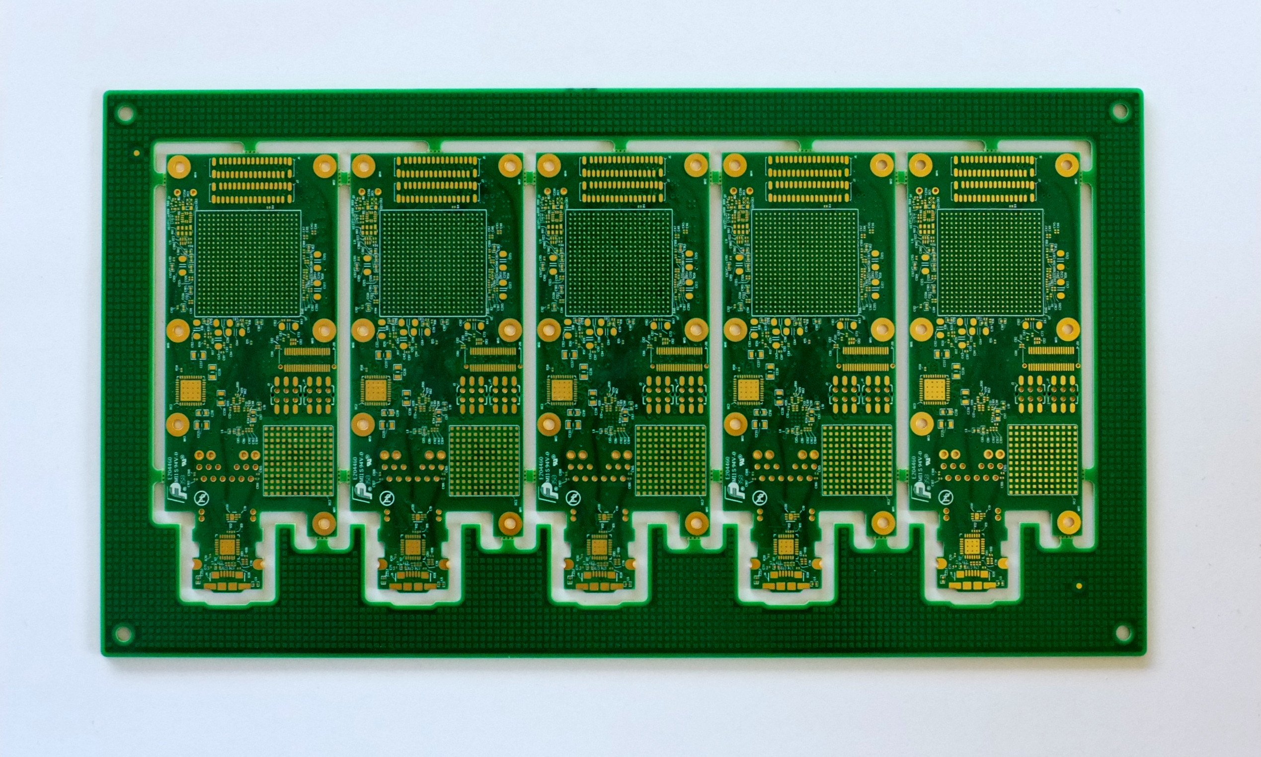
10393 System board, top side
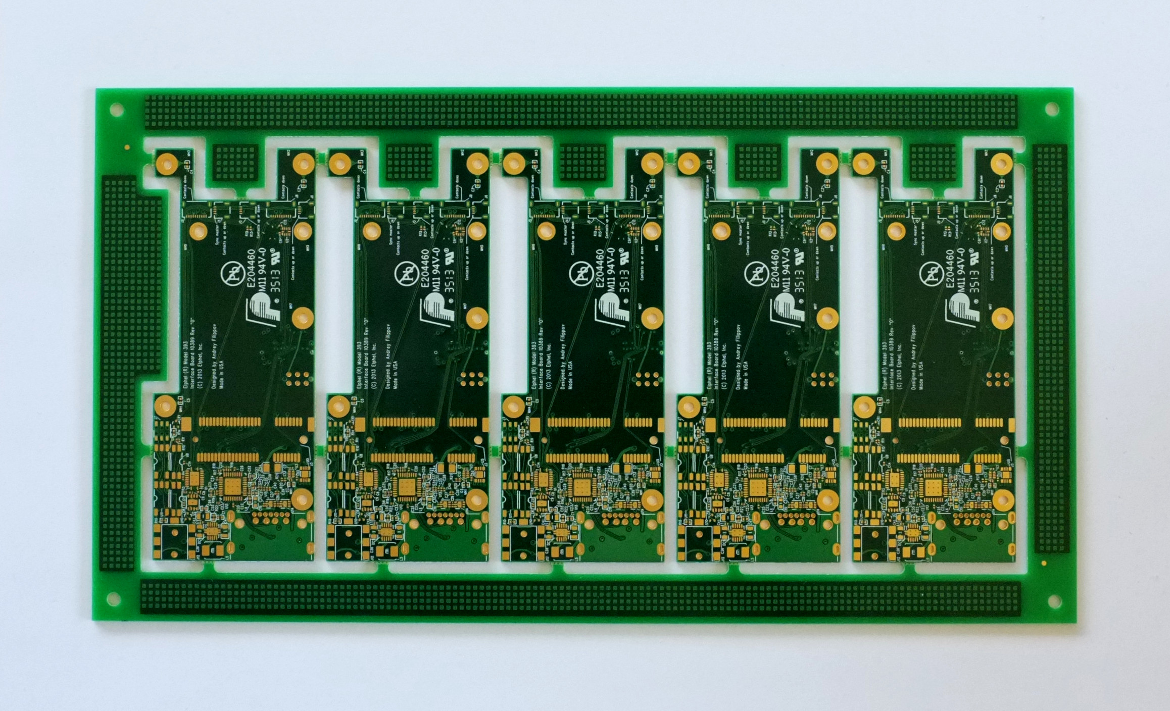
10389 Interface board, top side
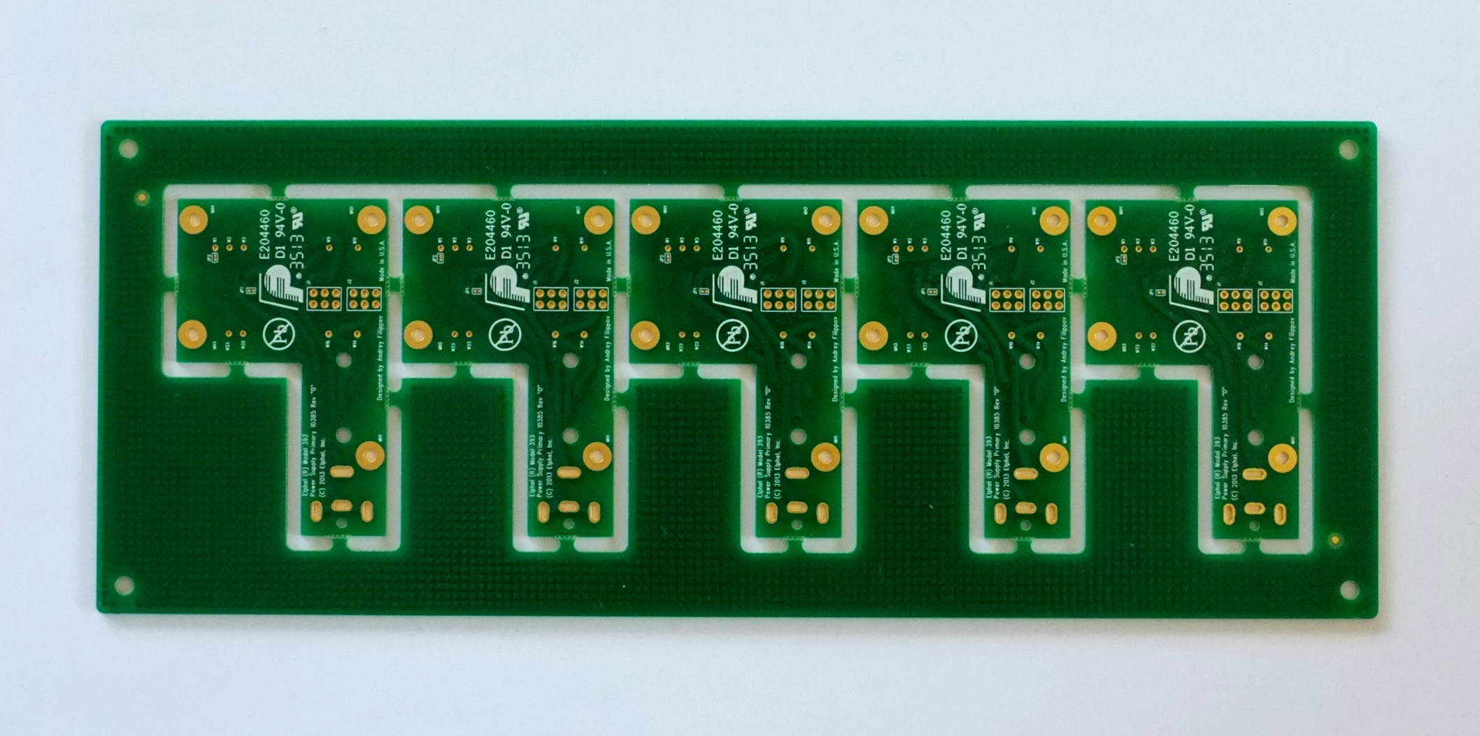
10385 Power supply board, top side
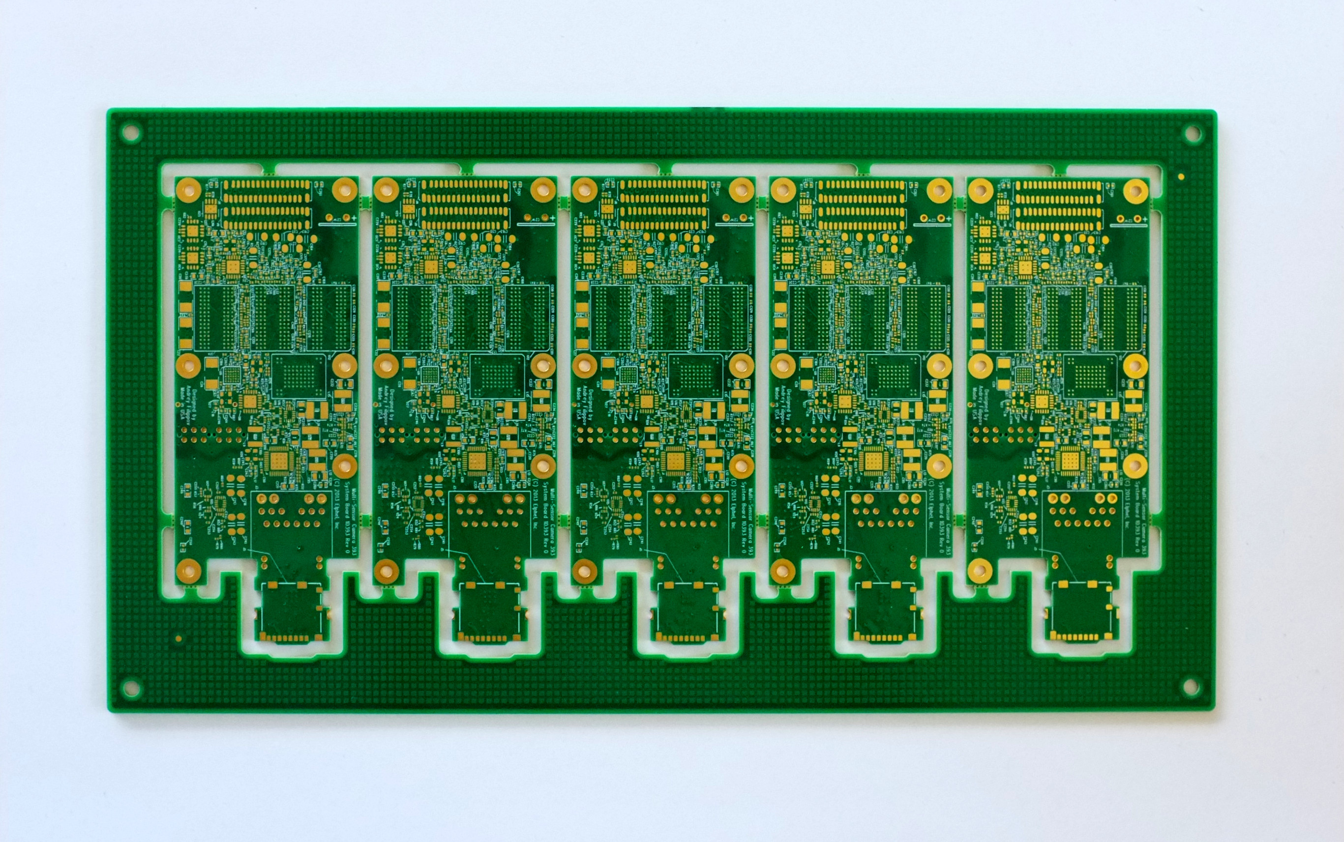
10393 System board, bottom side
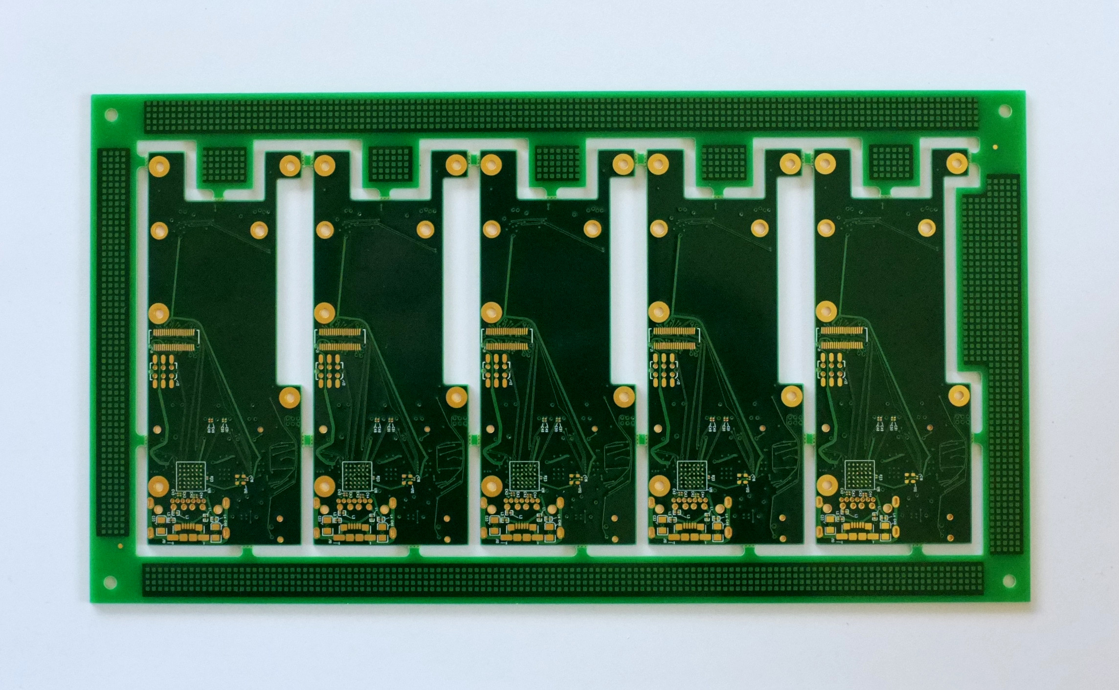
10389 Interface board, bottom side
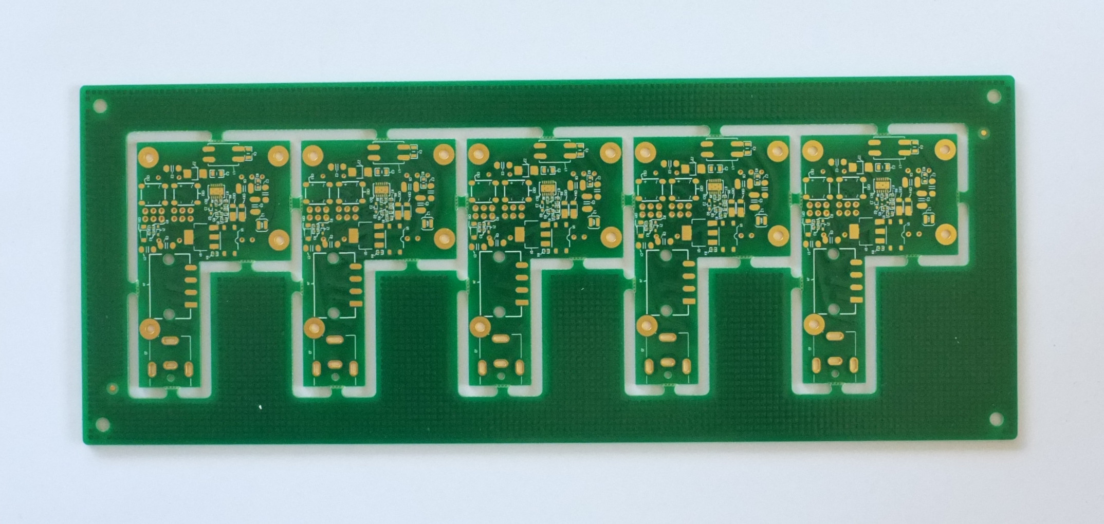
10385 Power supply board, bottom side
NC393 development progress – 2
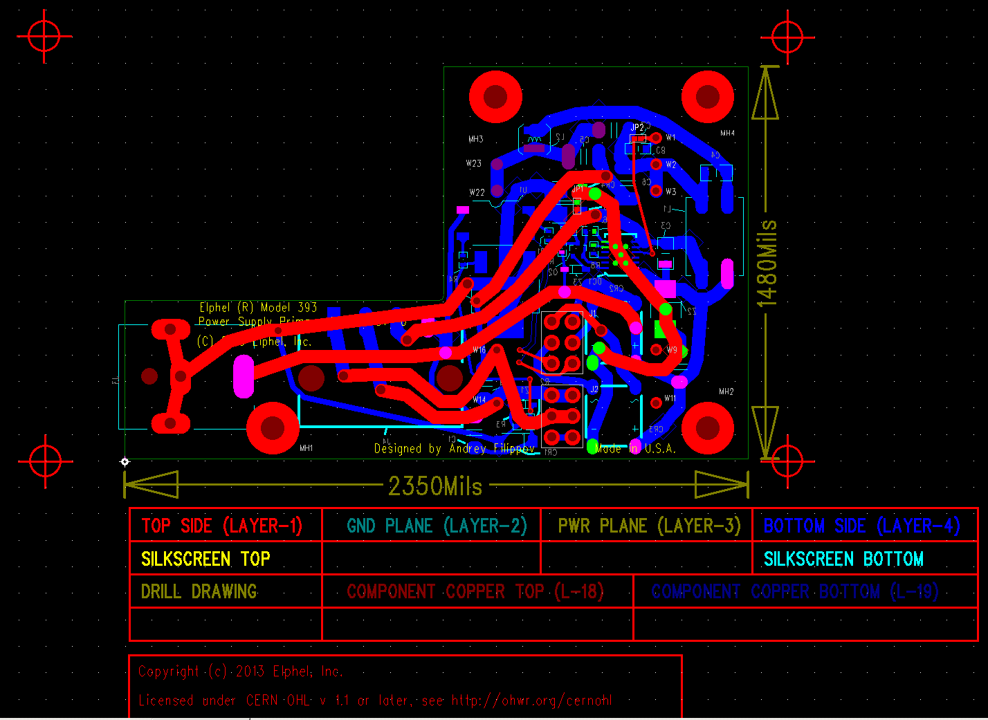
10385 – Power supply board layout
There is a small update to the previous post – circuit design and the PCB layout is done for the two companion boards. And it lead to some re-design on the system board. When working on the power supply board (it provides camera with the regulated 3.3V from the external source) I realized that it will have to hang on just two screws – not good for a rather heavy board with Traco DC/DC module (same size as the one currently used in Elphel NC353L camera). The 10393 system board and the 10389 Interface/SSD boards will be mounted on two sides of the aluminum heat sink plate (CNC-ed to match component heights) and the smaller 10385 will sit on top of the 10393, and all the 10385 mount screws have to go through the system board. So I had to add additional holes near the middle of the 10393. That in turn required to move the 40-pin inter-board connector that carries SATA, USB, synchronization and additional general purpose signals to the 10389. So I had to re-route part of the design, but it was a right time to do as none of the boards was released yet leaving the freedom for such modifications. These new holes will also improve the mounting of the heat sink to the Zynq chip (the large white square on the 10393 layout below).
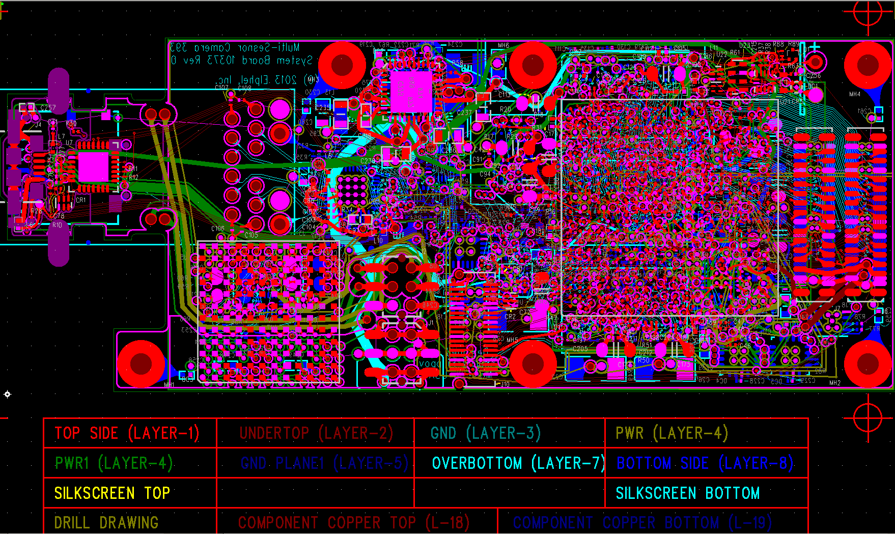
10393 – updated system board layout
Now when the core PCBs are designed (later will come new sensor boards and the successor to the current 10359 based on Xilinx XC7K160T to allow a single system board run up to 16 individual sensors), there is a boring part to double check all the pinouts and footprints of the new components, try to weed out as many other design errors as possible. Some will probably remain and will require re-spin of the boards, same as it was with our current camera. The 10353 system board is now revision “E” (6-th version), sensor board is also “E”, 10359 is “B” and the 10369 is “A”. But it will be very nice if the first prototype will be operational from the first attempt and the remaining bugs will not “brick” it completely, and we will be able to get enough information for implementing the needed changes. It did work this way before so I hope it will happen again. But still that boring part is ahead.
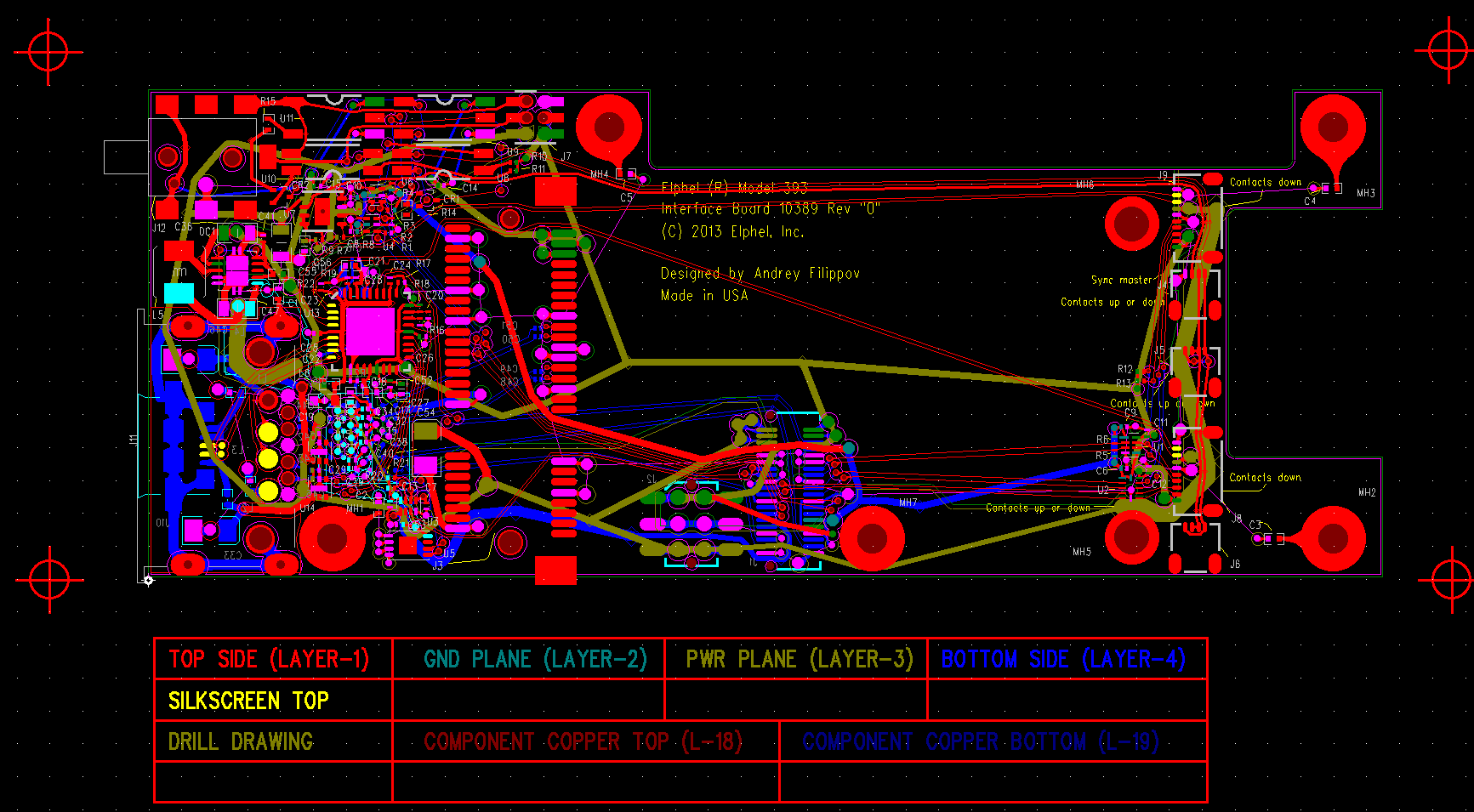
10389 – Interface/SSD board layout. Large part of the board is empty – this is the place for the SSD board
NC393 development progress
Development of the NC393 is now started, at last – last 6 weeks I’m working on it full time. It is still a long way ahead before the new camera will replace our current model 353, but at least the very first step is completed – I just finished the PCB layout of the system board.
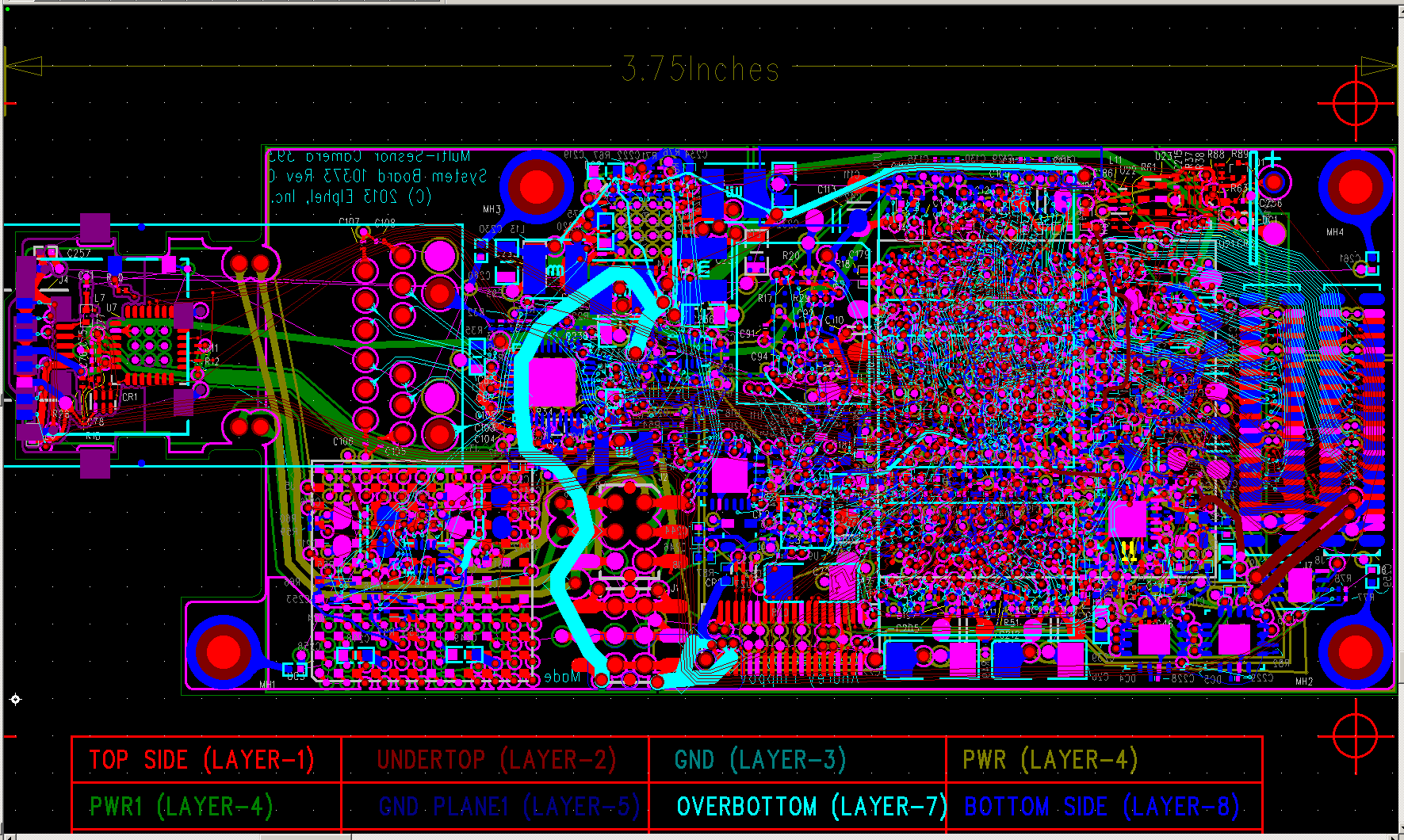
10393 System Board PCB layout
There were not so many changes to the specs/features that were planned and described in the October 2012 post, the camera will be powered by Xilinx Zynq SoC (XC7Z030-1FBG484C to be exact) that combines high performance FPGA with a dual ARM CPU and generous set of built-in peripherals. It will have 1GB of on-board system memory and 512MB of additional dedicated video/FPGA memory (the NC353 has 64MB each of them). Both types of memory consist of the same 256Mx16 DDR3 chips – 2 for the system (to use full available memory bus width of 32 bits) and one for the FPGA.
The main class of the camera applications remains to be a multi-sensor. Even more so – the smallest package of the Zynq 7030 device turned out to have sufficient number of I/Os to accommodate 4 sensor ports – originally I planned only 3 of them. These sensor ports are fully compatible with our current 5MPix sensor boards and with the existent 10359 sensor multiplexer boards – with such multiplexers it will be possible to control up to 12 sensors with a single 10393. Four of the connectors are placed in two pairs on both sides of the PCB, so they overlap on the layout image.
These 5MPix Aptina sensors have large (by the modern standards) pixels with the pitch of 2.2 microns and that, combined with good quality of the sensor electronics will keep them useful for many of the applications in the future. This backward compatibility will allow us to reduce the amount of hardware needed to be redesigned simultaneously, but of course we are planning to use newer sensors – both existent and those that might be released in the next few years. Thanks to FPGA flexibility, the same sensor board connectors will be able to run alternative types of signals having programmable voltage levels – this will allow us to keep the same camera core current for the years to come.
Alternative signals are designed to support serial links with differential signals common in the modern sensors. Each of the connectors can use up 8 lanes plus differential clock, plus I²C and an extra pair of control signals. These four connectors use two FPGA I/O banks (two per bank), each bank has run-time programmable supply voltage to accommodate variety of the sensor signal levels.
We plan to hold the 10353 files for about a month before releasing them into production of the prototype batch while I will develop the two companion boards. Not very likely, but the development of these additional boards may lead to some last-minute changes to the system board.
One of them – 10389 will have functionality similar to the current 19369 board – it will provide mass storage (using mSATA SSD), inter-camera synchronization (so we will be able to use these camera modules in Eyesis4π cameras) and back panel I/O connectors, including microUSB, eSATA/USB combo and synchronization in/out. The eSATA/USB combo connector will allow attaching the external storage devices powered by the camera. The same eSATA port will be reconfigurable into the slave mode, so the images/video recorded to the internal mSATA SSD will be transferred to the host computer significantly faster than the main GigE network port allows.
Another board to develop (10385) is the power supply – I decided to remove the primary DC-DC converter from the system board. Camera uses multiple DC-DC converters – even the processor alone needs several voltage rails, but internally it uses a single regulated 3.3V – all the other (secondary) converters use 3.3V as their input and provide all the other voltages needed. In the 10393 boards most secondary voltages are programmable making it possible to implement “margining” – testing the camera at lower and higher than nominal voltage and making sure it can reliably withstand such variations and is not operating on the very edge of the failure during the production testing. Primary power supply role is to provide a single regulated voltage starting form different sources such as power over the network, battery, wall adapter or some other source. It may need to be isolated or not, the input power quality may be different.
One reason to separate the primary power supply from the system board is that currently we have about half of the cameras made to be powered over the network, and another half – modified to use lower voltege from the batteries. Currently we order the 10353 boards without any DC-DC converter and later install one of the two types of the converters and make other small changes on the board. Some of our customers do not need any of the primary DC-DC converters – they embed the 10353 boards and provide regulated 3.3V to the modified 10353 board directly. Multi-camera systems can also share primary power supplies. This makes it more convenient to make a power supply as a plug-in module, so the system board itself can be finished in one run.
Another reason to remove the primary power from the system board is to remove the IEEE 802.3af (PoE) functionality. During the several last years we survived multiple attacks of the “patent trolls” (or NPE – non-practicing entities, how they like to call themselves), but we’ve spent thousands of dollars paid to the lawyers to deal with the trolls – some of the them tried to sell us the license for the already expired patents. One of the still active patents is related to “phantom power “- providing power through the signal lines, similar to how it is done for the microphones since 1919. To avoid the attacks of the trolls in the 10353 cameras we were able to use power over the spare pairs (Alternative B), but that is not possible with GigE which needs all 4 pairs in a cable. We do not believe that using this nearly century-old technology constitutes a genuine invention (maybe tomorrow somebody will “invent” powering SATA devices in the same way? Or already did?) but being a small company we do not have the power to fight in this field and invalidate those patents.
So the new NC393 made by Elphel will not have the PoE functionality, we will not make, manufacture, sell or market it (at least in GigE mode). But the camera will be PoE-ready, so as soon as the patent will become invalid, it will be possible to add the functionality by just replacing the plug-in module. And of course our cameras are open and hackable, so our users (in the countries where it is legal, of course – similar to installation of some of the software programs) will be able to build and add such module to their cameras without us.
Both of these companion boards are already partially designed so I plan that next month we will be able to release the files to production and start building the first prototype system. To test the basic functionality of the system board the two other ones are not needed – serial debug port (with the embedded USB-to-serial converter) is located on the system board, and 3.3V will be anyway originally provided by a controlled power supply. When everything will be put together the camera will get a well-known but still a nice feature for the autonomous battery-powered timelapse imaging: it will be able to wake itself up (using alarm signal from the internal clock/calendar that it has anyway), boot, capture some images and turn the power off virtually completely – until the next alarm.
Elphel new camera calibration facility
[caption id="attachment_4590" align="alignright" width="500" caption="Fig.1. Elphel new calibration pattern"] [1][/caption]
Elphel has moved to a new calibration facility in May 2013. The new office is designed with the calibration room being it's most important space, expandable when needed to the size of the whole office with the use of wide garage door. Back wall in the new calibration room is covered with the large, 7m x 3m pattern, illuminated with bright fluorescent lights. The length of the room allows to position the calibration machine 7.5 meters away from the pattern. The long space and large pattern will allow to calibrate Eyesis4π positioned far enough from the pattern to be withing depth of field of its lenses focused for infinity, while still keeping wide angular size, preferred for accuracy of measurements.
We already hit the precision limits using the previous, smaller pattern 2.7m x 3.0m. While the software was designed to accommodate for the pattern where each of the nodes had to have individually corrected position (from the flat uniform grid), the process assumed that the 3d coordinates of the nodes do not change between measurements.
The main problem with the old pattern was that the material it was printed on was attached to the wall along the top edge but still had a freedom to slightly move perpendicular to the wall. We noticed that while combining measurements made at different time, as most of our cameras need to be calibrated at several "stations" - positions relative to the target (rotation around 2 axes is performed automatically). We ran calibration during night time to reduce variations caused by vibrations in the building, so next station measurements were performed at different dates. Modified software was able to deal with variations in Z (perpendicular to the surface) direction between station measurements (that actually did help in the overall adjustment of variables), but the shape of the target pattern could change if the temperature in the building was changing during measurements. The PVC material has high thermal expansion, and small expansion in the X,Y directions could cause much higher variations perpendicular when the target is attached to the wall with lower thermal coefficient in multiple points.
[caption id="attachment_4646" align="alignleft" width="500" caption="Fig. 2. Floor plan"] [2][/caption]
Calibration Room
The new space is designed to accommodate various camera calibration procedures.
First of all we made the pattern as large as possible - it is 7,01m x 3.07m - we even raised the ceiling near the target.
The target itself is now printed on the film attached to the wall as a wallpaper, so there is no movement relative to the wall, and thermal expansion is defined by a lower coefficient of the drywall. We also provided the air channels inside the wall to make it possible to implement thermal stabilization of the wall.
The calibration room allows to move camera under test up to 7.5m away from the pattern, the room is separated from the rest of the facility with the wide "garage" door, so changing the lighting conditions outside of the room do not influence calibration.
Other rooms are designed in such a way that the camera can be moved up to 24 meters from the target (with the garage door open) and have unobstructed view of virtually the full pattern - that may be needed for the long focal length lenses.
[caption id="attachment_4598" align="alignright" width="500" caption="Fig. 3. Pattern wall during construction"] [3][/caption]
Preparing the wall for the target pattern
During construction of the new facility we were carefully watching the progress as our temporary space was located just on the next floor and we were mostly concerned about the quality of the target wall. Yes, software can accommodate for the non-flatness of the wall but it is better to start with the good "hardware" - to achieve subpixel precision the software averages correlation over rather large areas of the image (currently 64x64 pixels) so sharp variations will produce different measurements from different distances or viewing angles. When we first measured the wall flatness, we noticed large steps between the gypsum board panels, so the construction people promised to make it level 5 finish [4] and flatten the surface. They put "mud" all over the wall, sanded it and that removed all of the sharp discontinuities on the target surface, but still leaving some smooth ones up to ±3mm as we measured later with the camera.
When the wall was made flat it had to be prepared for application of the self-adhesive vinyl film, so the wall finish will not make it bubble later. Ideally we wanted it to be able to withstand peeling off the film if we'll have to do that. When we searched Internet about vinyl film application to the painted wall we found that most fresh paint needs some 60(!) days to cure before the film can be applied. So we decided to go with two-component epoxy paint that requires only one week before the film can be applied. When we inspected that epoxy painted wall (the paint was applied with the regular rollers) - it did not look flat. Well, it was just a roller-painted wall, so it had those small bumps and we were concerned that the vinyl film will conform to these bumps, and if it will - the position "noise" will be higher than what cameras can resolve. So we've got more epoxy paint and started a long process of wet-sanding and application of the new paint coats. We have compressed air (used to blow during optical and mechanical assembly) so we thought we'll just spray the paint instead of rolling it to avoid those bumps that were left even after professional work. Unfortunately, without the needed experience in spray-painting, we adjusted pressure too high, and probably as much as a half of our first coat ended somewhere else, but not on the sprayed wall - the paint droplets were too small. Next coat was better, and in several days we had a wall that seemed to be covered with hard plastic laminate, not just painted.
Installing the pattern
Our next concern was - how to install the vinyl film? We wanted to have very good match between the individual panels, as it is not possible to have the target printed on a single piece, maximal width of which is just over 1.5m. We hesitated to order professional installation because for regular applications (like vehicle wraps) such sub-millimeter precision is not required. For the really seamless (compared to the precision of the calibration) we needed better than 0.1mm match, but it is possible to just mask out the grid nodes around the seams and disregard them during calibration data processing, so we planned to get to about 0.5mm match.
[caption id="attachment_4616" align="alignleft" width="500" caption="Fig.4. Pattern Z-deviations (perpendicular to the target plane)"] [5][/caption]
[caption id="attachment_4591" align="alignleft" width="500" caption="Fig. 5. Pattern deviations in X,Y plane"] [6][/caption]
[caption id="attachment_4619" align="alignleft" width="500" caption="Fig. 6. Pattern deviation from the "ideal" grid (horizontal profile)"] [7][/caption]
We knew people are doing that but still it seemed very difficult to apply 1.5m wide by 3m long "stickers" without wrinkles and bubbles. Web search provided multiple recommendations, but the main thing was to use "wet" method that none of us new before. It involves spraying the wall (and the film on the adhesive side) with "application fluid" (basically water with small addition of soap and alcohol). When the sticky film is applied to the wet surface, the adhesive is temporarily inhibited and it is possible to reposition (slide) the film to achieve required match. Then the water is squeezed away with the squeegee [8] tools, and if done properly, there should be no bubbles left.
Geometric properties of the pattern
The Z-deviations on Fig. 4 show the wall non-flatness, the gypsum panel borders are still visible (even with "level 5" finish), the horizontal discontinuity near the top is where the wall was extended to accommodate increased ceiling height. Positive Z direction is away from the camera, so lighter areas are concave areas on the wall and darker are bumps extending out from the wall.
Fig.5. illustrates mismatch and stretching of the vinyl panels application. Red/green color difference corresponds to the horizontal shift, while blue/green - the vertical one.
Figure 6. contains a horizontal profile at the half-height and provides numerical values of the deviations. Diff. Error plot indicates areas around panel boundaries that should be avoided during reprojection errors minimization and measuring point spread functions (PSF) for aberration correction.
Illuminating the target pattern
We use the same pattern for different parts of the camera calibration. Correction of aberrations and distortions does not impose strict requirements on the illumination of the pattern, but we use the same images to measure (and compensate) lens vignetting and color variations of the camera sensitivity caused among other reasons by the multilayer infrared cutoff filter and angular variations of the pixel color sensitivity. This method works for low-frequency part of the flat field correction and does not deal with the pixel fixed-pattern noise that, if present should be corrected by other means.
[caption id="attachment_4592" align="alignright" width="400" caption="Fig. 7. pattern brightness for station 2 view 0 (top channels) "] [9][/caption]
[caption id="attachment_4593" align="alignright" width="400" caption="Fig. 8. pattern brightness for station 2 view 0 (top), specular component"] [10][/caption]
[caption id="attachment_4594" align="alignright" width="400" caption="Fig. 9. pattern brightness for station 2 view 1 (bottom channels)"] [11][/caption]
[caption id="attachment_4595" align="alignright" width="400" caption="Fig. 10. pattern brightness for station 2 view 1 (bottom channels), specular"] [12][/caption]
Acquiring thousands of images made by different channels of the camera and capturing the same target, it is possible to perform simultaneous relative photometric calibration of the pattern and the sensors, provided that each element of the pattern preserves the same brightness for each image where it is captured. This may be true when the target is observed from the same point, but when we calibrate Eyesis4π camera with 2 sensors attached far from the other ones, and these sensors travel significantly when capturing the target, this assumption does not hold. The same pattern element has different brightness depending on the lens position when the image is acquired. This is because even matte pattern material is not perfectly diffusive, there is some specular (reflective) component.
In the earlier setup we used photographic lamps with large umbrellas, but these umbrellas were still small when placed at a distance that they were out of the camera view. Specular component was still visible when the diffusive part was subtracted. When designing the new calibration target we decided to use bright linear fluorescent lamps along the floor and the ceiling and keep them spatially compact without any diffusers or umbrellas, we only used mirrors behind the lamps to effectively double the output. Such light source was expected to produce specular reflections on the target, but these reflections occupy just a small portion of the target surface, the rest of it is close to be pure diffusive. That allowed us to locate positions of the specular reflections for each camera station/viewpoint by subtracting the average (between all stations/viewpoints) pattern brightness from each individual station/view of the pattern and then masking out this areas of the pattern during flat-field calculations.
Images on Fig. 7-10 were made for camera station 2 - 3.3m from the target and 1.55m to the right of the target center, that caused lamp reflections to be shifted to the left. View 0 (Fig. 7-8) correspond to the camera head, which is the center of rotations. View 1 (Fig. 9-10) is captured by the camera 2 bottom sensors mounted 820 mm below the camera head, so they were moving significantly between the images - that caused visible curvature on the top lamps reflection.
Virtual tour of Elphel calibration facility
You may walk through [13] our calibration facility using our WebGL viewer/editor. The images were captured with newly calibrated Eyesis4π camera, there is no 3-d parallax correction - these are just raw panoramas stitched for infinity and most close objects are out of depth-of-field of the lenses. Hope you'll still enjoy this snapshot of the new facility were we plan to develop and precisely calibrate many new cameras.
[1] http://blog.elphel.com/wp-content/uploads/2013/06/wall_color.jpeg
[2] http://blog.elphel.com/wp-content/uploads/2013/06/floor_plan.png
[3] http://blog.elphel.com/wp-content/uploads/2013/06/DSCF8109-wall.jpg
[4] http://nationalgypsum.com/resources/tech-talk-revisiting.htm
[5] http://blog.elphel.com/wp-content/uploads/2013/06/c13ff-grid-difference-Z-rotated-4x-cropped.png
[6] http://blog.elphel.com/wp-content/uploads/2013/06/c13ff-pattren-difference-XY-color.png
[7] http://blog.elphel.com/wp-content/uploads/2013/06/diff-XYZ-profile-nohead.png
[8] https://en.wikipedia.org/wiki/Squeegee
[9] http://blog.elphel.com/wp-content/uploads/2013/06/c13ff-station2-view0.png
[10] http://blog.elphel.com/wp-content/uploads/2013/06/c13ff-station2-view0-specular.png
[11] http://blog.elphel.com/wp-content/uploads/2013/06/c13ff-station2-view1.png
[12] http://blog.elphel.com/wp-content/uploads/2013/06/c13ff-station2-view1-specular.png
[13] http://community.elphel.com/files/eyesis/pano-db-3/webgl_panorama_editor.html?kml=20130517_ro.kml
Sensor+Lens Tool
[1]
There's a number of online lens calculators already and this one is not conceptually different - the focus is on the current sensor we use and the main feature is visualization done in HTML canvas [2] using jCanvas [3].
It might help to figure out what lens is needed for a particular application where certain parameters can be important, e.g.:
Field of view for a lens of the given format
Depth of field at a fixed distance and f-stop
Aperture size (f-stop) at which the resolution starts to degrade due to diffraction limiting
The tool covers:
Different sensor formats (also compared to the "full frame" format)
Circle of confusion formulae (affects hyperfocal distance and depth of field):
1px - for machine vision applications
d/1730 & d/1000 - "Zeiss formula [4]" for photography
Distance to in-focus plane
Lens focal length
Field of view
Diffraction limit for aperture size (calculated for red light of 690nm, Airy disk [5] size equals to 1px)
Depth of field
Links
Sensor+Lens Tool [6]
[1] http://community.elphel.com/files/dof/
[2] http://www.w3schools.com/tags/ref_canvas.asp
[3] http://calebevans.me/projects/jcanvas/index.php
[4] http://en.wikipedia.org/wiki/Zeiss_formula
[5] http://en.wikipedia.org/wiki/Airy_disk
[6] http://community.elphel.com/files/dof/
Heptaclops camera and the 393
"Temporary diversion" that lasted for three years
[1]Last years we were working on the multi-sensor cameras and optical parts of the cameras. It all started as a temporary diversion [2] from the development of the model 373 cameras that we planned to use instead of our current model 353 cameras based on the discontinued Axis CPU. The problem with the 373 design was that while the prototype was assembled and successfully tested (together with two new add-on boards) I did not like the bandwidth between the FPGA and the CPU - even as I used as many connection channels between them as possible. So while the Texas Instruments DaVinci processor was a significant upgrade to the camera CPU power, the camera design did not seem to me as being able to stay current for the next 3-5 years and being able to accommodate new emerging (not yet available) sensors with increased resolution and frame rate. This is why we decided to put that design on hold being ready to start the production if our the number of our stored Axis CPU would fall dangerously low. Meanwhile wait for the better CPU/FPGA integration options to appear and focus on the development of the other parts of the system that are really important.
Now that wait for the processor is nearly over and it seems to be just in time - we still have enough stock to be able to provide NC353 cameras until the replacement will be ready. I'll get to this later in the post, and first tell where did we get during these 3 years.
Optical measurements, mechanical design, image processing and cameras calibration
Up until 2009 we did not really bother with the optics of the cameras we made - cameras have a standard CS-mount that can accommodate C- and CS-mount lenses, available from many suppliers. We provided the electronics and software, but it was up to our users to deal with the rest. Yes, we did offer cameras with color and monochrome sensors, with or without IR cutoff filters, stocked some basic varifocal lenses - but that was virtually all. When we started to develop panoramic cameras ourselves we quickly recognized that the lenses we need just do not exist. The C/CS-mount format lenses are too big to make a compact layout of the camera (it not only becomes big itself, but large distance between the lenses cause large parallax that makes panorama stitching more difficult). The smaller M12 mount lenses (also called "S-mount", and "board lens") are mostly designed for the small security cameras and being cost-sensitive are not usually designed for the top performance.
We also realized that putting together multiple individual cameras to cover a panorama is not enough. All camera lenses have best resolution in the center, while closer to the corners it degrades. In many, especially small lenses the corners are substantially darker due to vignetting. And while we got used to it making photographs - in many cases it was even be considered as a useful feature to focus on the object in the center and blur and fade out the periphery, in stitched panoramas it is a disaster, as the individual lenses peripheral areas will be mapped to the middle areas of the composite panorama image.
Not being the lens manufacturers ourselves we went the path of correcting the lens aberrations by software post-processing ( "Zoom in. Now… enhance." [3] and later posts) - that allowed us to effectively double number of lens "megapixels". Later we used the same pattern we developed for aberration correction to precisely correct the lens distortions. This process of camera calibration for the spherical view camera is described in my previous blogs (such as Building and Calibrating Eyesis4π [4]) - we started to do so for the precise panorama stitching but later worked on making it suitable for the stereo photogrammetry and 3d reconstruction.
So now we have what we believe is the highest performance camera of a kind - the one that we demonstrated at SIGGRAPH-2012 [5]. We also have now precise thermally-compensated sensor front end that can be used in other applications - in an individual camera or in multi-camera setups.
One such application is
Shallow depth of field and cinema cameras
For many years now Elphel was cooperating with a group of enthusiasts who tried to adapt our cameras to use for cinema applications - and that fits very well into our vision: take our cameras and use them as clay to form something you (not us) envision. But eventually they got tired of waiting for our next model 373 camera (that they needed to support higher frame rate and larger image sensor) so they decided to develop a new camera themselves.
One of the main camera features they (and others who are interested in the cinematographic applications) needed was the physically large sensor. Such sensors allow capturing images with "shallow" depth of field (DoF) and can be used to shoot video where some objects are in focus, while others (farther or closer) need to be blurred. With the single lens systems the scale of distances where you can use DoF depends on the physical size of the sensor and with the small sensor as we use (and those used in camera-phones) are approximately 5 times (linearly) smaller than the 35-mm film frame. So what you can achieve with 35mm camera in 5-10 meter range is only possible in the 1-2 meter range with the small 1/2.5" (~7mm diagonal) sensor - so instead of the human actors you'll have to make animation with dolls. There are even special optical adapters [6] that use 35mm format lens to focus image on the diffusing screen (made of wax or even fast rotating disk to make diffusing grains smaller) and then transfer the image on that screen to the small format sensor of the inexpensive camcorder. But that system still had limited resolution and was loosing a lot of light, dramatically reducing the camera sensitivity.
[caption id="attachment_4440" align="alignleft" width="500" caption="Three-camera setup for controlled depth of field capturing"] [7][/caption]
The DoF first came as the feature inherent to the physical camera, the process of capturing the three-dimensional world on a two-dimensional media (film or image sensor). But in the artist's hands it became a tool to focus viewer attention on the intended objects and also to show the 3-d nature of the actual world. With the modern computer animation there are no physical cameras with the lenses involved, but the depth of field is still present (like in this Sintel gallery [8]). That means that the "shallow" DoF can be synthesized when the 3d information about the scene is present, and such information can be captured by other means - not only by the large format sensor and then the result image is rendered with synthetic depth of field. In some cases even a stereo-camera setup (a pair of synchronized cameras) can be used. Such setup is generally sufficient, if the in-focus objects are in foreground and there is nothing closer to the camera that occludes the target. But if such system is used to capture say image of a human behind the tree branches, then a single horizontal branch can close view of the human eye to both camera lenses. So regardless of how you blur the foreground objects (tree branches in this case) you will not be able to reconstruct the sharp image of the human face - there is no information about the color of the eye completely missing on both camera images. Using more cameras in the setup helps to provide more information about the objects - in our last case the third camera shifted vertically from the first two will have the information about the eye that was missing on the images from the first two cameras.
Building the 3-d model of the scene from the multiple images is not an easy task. The precision of the depth measurements is much lower than measuring distances in the direction orthogonal to the line of view. And often the portions of the scene have no fine details and so there is nothing to match to find out the distance to that object. On the other hand, when the 3-d reconstruction is needed just for synthesizing DoF, the precision of the distance needed to simulate the DoF of a real lens is the same as you can get from the lenses separated by the large lens diameter. The areas that do not have details, where it is impossible to measure distance - that areas would look the same on the final image, even if you blur them with the wrong sigma (or not blur at all).
HTML5 demo
[caption id="attachment_4465" align="alignright" width="420" caption="A section of the screenshot - click on the image to open the actual HTML5 demo page"] [9][/caption]
We do not yet have a seven-camera setup or "heptaclops", we used a smaller "triclops" configuration. When we had built and calibrated the new camera (using the target pattern data measured earlier with Eyesis) we looked at the way to demonstrate it. First the images were processed with the known calibration and each of the raw images was mapped to the common projection plane - each pixel with ~0.15 pix accuracy - this process compensates for the lenses distortions and mis-alignment of the individual sub-cameras. These images can be used as the input data for the 3-d reconstruction. We do not have finished 3-d processing software yet, Oleg Dzhimiev [10] made a small HTML5 application [11] that illustrates the information from the camera triplet.
This web application overlaps the triplet of the corrected images acquired simultaneously by the 3 sub-cameras and applies the transparencies to the two of them so the the visible superposition has equal weight of each image of the set. Then each image is shifted by the value of the disparity that matches the distance from the camera to the image plane - the amount of disparity is controlled by a slider or by rotating the mouse scroll wheel. The objects in or near the selected image plane from all three images coincide, while the objects closer or farther from the camera are shifted from each other. When the shift is small, it looks like a blur, but farther images look as they actually are - as individual ones. While these separate image spoil illusion of the out-of-focus blurring (but still looking more realistic than dual images in old rangefinder cameras [12]), they illustrate the raw data. Using more parallel cameras would improve illusion of focusing on such fast demo and provide more data for the actual reconstruction, reduce ambiguity when finding the disparity (and so the distance) at each pixel. Additionally, combining the data from multiple individual sensors would increase signal-to-noise ratio of the result image and so the dynamic range even if used with the same exposure/gain settings. And it is possible to program some channels with different exposure and run the whole system in the HDR mode.
The same applcation can be useful with the 3-d processing too. Instead of the 3 images that are just aberration and distortion corrected originals acquired from the different sensors, we can generate multiple close views and feed them to the same program - just shifting multiple images (or videos) is much less computationally demanding as correct 3-d rendering of the scene with the selected image plane and DoF, so such application can be used as a preview for the artist to dynamically adjust those parameters (distance and DoF) before running the final rendering (when it is possible to add desired bokeh [13] too).
Back to the Model NC373 camera status
[caption id="attachment_4441" align="alignleft" width="400" caption="Model NC393 CAD rendering with M12 (S-mount) lens and thermally compensated sensor front end"] [14][/caption]
We decided to drop the idea of building the already designed and prototyped model NC373 camera. While the next camera will share some parts with the 373, the changes are too big to call it just a revision "C" of the 10373 system board, so it will be model NC393. The camera system board will have Xilinx Zynq that combines FPGA and a dual-core ARM processor on a same chip, so my main concern of the FPGA-CPU bandwidth is not applicable here.
When information about the new Xilinx device was announced, I thought it is a good candidate for the next camera design. In spring of the last year we had a Xilinx seminar in Salt Lake City, where I was told that these new devices will be supported by the zero-cost development software.
[caption id="attachment_4442" align="alignright" width="400" caption="Model NC393 CAD rendering with a C/CS-mount lens"] [15][/caption]
That feature is very important for us, because while the cost of the tools is not high for the manufacturer, it is higher than the cost of a camera. We strive to make our products highly customizable by the users, each camera contains the source code needed to compile the executables (including the FPGA code). Making our customers to pay high price to be able to modify even a single line of the FPGA code is not acceptable to us, so we use only those FPGA devices in our designs that are supported by the software that our users can download at zero cost. Of course ideally we would love to use free (FLOSS) development tools (like we use for the FPGA functional simulation), not just the zero cost ones, but in the real world it is not possible yet, so we develop and share our free (licensed under GNU GPLv3) code with the non-free closed-source tools.
The news that came from the Xilinx reps later last year were really disappointing - none of the Zynq devices (even the smallest one) will be supported by the zero-price software tools. And only this year it finally became official that 3 of the 4 devices is going to be supported and so we can use them. Xilinx did have some production delays, the availability schedule slipped to later dates, but I'm crossing my fingers that the needed part/package combination will actually be in production by the end of the Q1 2013.
[caption id="attachment_4444" align="alignleft" width="400" caption="Model NC393 CAD rendering with three M12 lenses and thermally compensated sensor front ends"] [16][/caption]
While the NC393 design is far from being finished, some features are already settled and are likely to remain unchanged in the final product.
The camera will be compatible with both parallel output sensors (such as the Aptina MT9P001/MP9P031/MP9P006 that we use currently) and the multi-lane serial sensors (such as having MIPI). The connectors will not change and the sensors used with NC353 will fit directly to the NC393 camera
The camera system board is being designed for the multi-sensor operation. It will accommodate three sensors without the need to use multiplexer boards (like 10359 [17] needed for NC353). Multiplexer boards will likely still be used in some cases, but the system board itself will have 3 identical sensor board connectors
Physical dimensions of the camera and the mounting holes location on the system board will remain the same as on the previous camera models
Camera will have a single GigE port as a main communication channel
One serial console port with internal USB converter, so a microUSB cable will be sufficient to use system console for the software development.
Firmware installation and update will be done by booting from the microSD accessible without opening of the camera. It will be possible to use the same card slot during normal operation for data storage.
512MB NAND flash as a main storage for firmware, boot source for camera normal operation.
1GB of the system memory made of the two 256x16 DDR3 chips.
512MB of dedicated video memory (not shared with the CPU) - one 256x16 DDR3 chip, same the one used for the system memory.
USB2 (host): One external micro-USB and 2 internal flex cable connectors with USB, additional 3.3VDC power, I2C and FPGA general purpose I/O compatible withe the add-on boards for the NC353
30-pin board-to-board connector with 12 differential /24 single-ended FPGA I/O for add-on boards.
a pair of 2.5mm audio connectors on the back panel for camera synchronization - from external trigger and/or from other cameras
2-port SATA controller based on the free (GNU/GPL) implementation [18]. Camera will have eSATA/USB external connector (so capable of running external SATA device without additional power supply) and internal mSATA SSD that fits inside the camera.
[caption id="attachment_4443" align="alignright" width="263" caption="Model NC393 CAD rendering with three M12 lenses for capturing panorama images"] [19][/caption]
NC393 camera will have significantly higher performance than the 353 and it will inherit the openness and flexibility from its predecessors. Elphel does not take orders on the custom design, but rather we try to do our best in making sure our users can do the customization themselves. The same policy would remain the same for the NC393 too - we will offer some camera options and add-ons, and in most cases it will be up to the camera users to build the camera of their dream.
Elphel will use the new system board in the Eyesis cameras. It will allow us to make the overall design more compact by reducing number of boards inside, increase the network bandwidth as well as the SSD bandwidth, increase the frame rate. We also plan to increase the camera resolution by switching to the same format but smaller pixel sensor while reusing the same optical-mechanical design - that would be definitely too much for the current system that is limited to the currently used sensors.
And of course we will continue to build "small" cameras based on the new design - with universal C/CS-mount and with M12 one, including precisely calibrated fixed-lens systems. And as the camera is designed for the multi-sensor operations, we will offer several typical configurations for robotic (parallel sensors for stereo-vision) and panoramic applications, as shown on the images above.
All the camera hardware documentation (circuit diagrams, parts lists, PCB layout and mechanical CAD files) will be released under CERN OHL license when the design will be finished and we will start the actual production of the cameras (add-on documentation will be released when it will become available) . All the firmware and FPGA code will be traditionally released under GNU GPL and maintained at Sourceforge repositories.
[1] http://blog.elphel.com/wp-content/uploads/2012/10/heptaclope.png
[2] http://blog.elphel.com/2009/11/temporary-diversion/
[3] http://blog.elphel.com/2010/11/zoom-in-now-enhance
[4] http://blog.elphel.com/2012/09/building-and-calibrating-eyesis4%cf%80/
[5] http://blog.elphel.com/2012/08/the-last-chance-to-see-us-at-siggraph12/
[6] http://en.wikipedia.org/wiki/Depth-of-field_adapter
[7] http://blog.elphel.com/wp-content/uploads/2012/10/triclope_2.jpeg
[8] http://www.sintel.org/gallery/
[9] http://community.elphel.com/files/phg3/index.php
[10] http://blog.elphel.com/category/oleg/
[11] http://community.elphel.com/files/phg3/index.php
[12] http://en.wikipedia.org/wiki/File:Rangefinder_window.jpg
[13] http://en.wikipedia.org/wiki/Bokeh
[14] http://blog.elphel.com/wp-content/uploads/2012/10/393-m12.png
[15] http://blog.elphel.com/wp-content/uploads/2012/10/393-cs-mount.png
[16] http://blog.elphel.com/wp-content/uploads/2012/10/393-triclope_25.png
[17] http://wiki.elphel.com/index.php?title=10359
[18] http://opencores.org/project,sata_controller_core
[19] http://blog.elphel.com/wp-content/uploads/2012/10/393-pano.png
Building and Calibrating Eyesis4π
This is a long overdue post describing our work on the Eyesis4π camera, an attempt to catch up with the developments of the last half of a year. The design of the camera started a year before that and I described the planned changes from the previous model in Eyesis4πi [1] post. Oleg wrote [2] about the assembly progress and since that post we did not post any updates.
Sensor front end challenges
Working on the first camera of this series we had to solve several technical problems - and that push us back behind our schedule. First problem was with the use of the UV-curing adhesive to fix the sensor relative to the lens. In the first Eyesis we incorporated some elements of the sensor adjustment into each SFE [3] (sensor front end), in the current system we decided to follow a more traditional approach and adjust the sensor on a specialized device and then fix the position with the adhesive - that allowed us to make the SFE more compact and we hoped to simplify it too. In the new design I tried to reduce the thickness on the UV-curable adhesive and make the system self-compensating for the glue shrinkage during curing and thermal expansion of it when the camera is used. The solution used 3 pins in 3 holes with the glue between the pins and the walls of the holes, so expansion/contraction of the adhesive would not lead so significant movement of the pins. Unfortunately the illumination of the glue with the UV radiation proved to be insufficient (some shadow areas remained) and the UV LED were on the same side of the glue where it contacted the air, so the most illuminated areas suffered from the "oxygen inhibition". We tried several small modifications but still could not achieve reliable and strong bonding we needed. So we decided to use just low-shrinkage epoxy instead of the UV glue the first camera and leave more radical redesign for later time. With epoxy we could make only 2 SFE in 24 hours, because the curing took much longer than the UV glue and we could not use fast-setting epoxy as the adjustment took some time. That method was slow but it worked. Worked until we decided to measure the temperature dependence of the focusing and realized that just maintaining the SFE "in focus" over the intended temperature range is not sufficient for our application where we compensate for the lens aberrations with post-processing. The measured temperature coefficient was about 0.2μm/°C - that corresponds to 10 mm of the expanding aluminum - material used in most of the SFE.
Thermally compensated SFE design
[caption id="attachment_4068" align="alignright" width="489" caption="Section of the SFE used in Eyesis4π"] [4][/caption]
We could not think of any quick fix to that problem so we decided to go through the complete redesign of the sensor front ends used in Eyesis4π cameras, add thermal compensation and improve bonding process. Some elements of the SFE are made of invar [5] - nearly zero expansion material for the thermal compensation, the bonding is spit into two separate stages - fast UV bonding and final using low-shrink epoxy. Additionally we modified the 10338D sensor front end PCB [6] (the new version has revision "E") to include the temperature sensor. Luckily for us we just had to replace a single chip - instead of the serial EEPROM the new board uses a combination of the EEPROM and a temperature sensor in the same size package and pinout (such chips are used in computer memory modules to store module parameters and monitor temperature). The new board simplifies temperature dependence measurements of each SFE during manufacturing, it also makes possible to do perform additional thermal correction of the acquired images - the SFE temperature during acquisition is embedded in the Exif header of each of them.
The 0353-07-25 SFE has two major parts - the base with the attached lens and the movable (during adjustment) plate to which the sensor PCB is attached. These two parts are connected with the 3 invar rods, each being press-in (and then flared) in the base. Only the very bottom part of the rod is press-fit, most of it is loose so the thermal expansion of the aluminum base is isolated from the rod. The base has 3 arms that are partially cut through to allow some bending, these arms support the invar rods laterally while allowing the axial movement caused by the thermal expansion. The top of each invar has aluminum cap pressed on and flared, these caps fit (with the sufficient clearance to guarantee co-contact during adjustment process) inside the holes in the sensor plate and are later bonded with the epoxy compound. Each of the 3 arms that provide lateral support of the invar rods additionally have 3 through holes that are temporarily plugged at the bottoms with the transparent adhesive tape to hold UV-curable adhesive. The sensor plate has 3 thin-wall stainless steel tubes pressed in it, these tubes are immersed in the adhesive and bonded to the base arms when irradiated with UV from the bottom during curing. The SFE is mounted in the adjustment machine with the lens pointed down, the mirror mounted at 45 degree reflects the target pattern located on the vertical wall. The same mirror reflects the UV radiation during curing process after the adjustment is finished. The 2.8mm invar spacer ring (for expansion it is in-series with the rods) is designed to slightly over-compensate the thermal expansion of the aluminum parts, so it can be made of different material (or a combination of 2 washers made of different materials) to fine-tune the overall expansion. This design allowed to reduce the thermal variance of the distance between the sensor and the focal plane of the lens by nearly an order of magnitude - the measured value falls in ±0.03 μm/°C range.
SFE compensated for the purpose of the aberration correction that maintains the same position of the lens focal plane relative to the sensor surface still has some magnification variations caused by the sensor expansion itself among other factors. It is not large - until we upgrade camera to the higher resolution sensors the change for 10°C is only 0.08 pixels for the diagonal corners of the image, this effect can be easily compensated when the temperature during acquisition is known.
Camera calibration machine
[caption id="attachment_4088" align="alignright" width="500" caption="Goniometer with Eyesis4π camera"] [7][/caption]
Camera calibration involves the following procedures:
measuring the point spread function (PSF) [8]for each area of the field of view of each sensor to be able to compensate for the aberration during post-processing of the acquired images
measuring distortions of each lens and precise orientation and position of each lens in the camera assembly so the result images have the pixels precisely mapped to the lines in space
measuring the vignetting [9] of each lens including variations of color reproduction over the area of each sensor
logging the inertial measurement unit (IMU) data
All the optical measurements (first three) are made with the same target pattern described in the earlier post [10]. When performing the distortion measurements the camera can be located rather close to the pattern, but for the aberration measurement and correction it should be within the depth-of-field range from infinity - distance at which the camera will operate. In our case it is 6 meters. With the individual sub-camera FOV of 45°x60° the target pattern would have to be 5m (horizontal) by 7m (vertical) to fill the sensor completely. As it is not easy to make and use such large target we developed software to combine PSF data from multiple overlapping images of a smaller pattern - we used 3022mm by 2667mm that fits on the wall in our office.
[caption id="attachment_4087" align="alignleft" width="500" caption="Calibration pattern"] [11][/caption]
When calibrating the earlier Eyesis model that had just 9 sensors we manually rotated the camera on a photographic tripod and were making at least 12 shots for each sensor. For the Eyesis4π with full sphere FOV and with the long tube body that can not be detached during calibration (it has essential electronic boards and the two bottom sensors on it) the regular tripod would not work. So we had built a special device that allows rotation of the camera around to axes - horizontal (it goes approximately through the center of the camera optical head) and the vertical axis of the camera. As the camera is capable to view at nadir (along the tube body) the camera is rotating in the polyurethane rollers that do not block the view of the target along the tube.
When the PSF are calculated during post-processing it does not matter what part of the pattern is visible - the ideal pattern is locally distorted for the best fit with the acquired images and then used in deconvolution to calculate the aberration correction kernels, minor geometric errors in the pattern and non-flatness of the pattern surface are not critical. But the same is not true when we perform the distortion measurements and precise pixel mapping - in that case the stretching of the pattern panels, non flatness would cause significant errors. In this case the pattern is treated as a 3-d mesh of the pattern cells with arbitrary coordinates of each of the nodes, these coordinates are determined during bundle adjustment with the camera parameters. The post-processing in this case should not just fit ideal pattern to the measured images, but have an absolute match (same cell to the same cell) between the wall pattern and the acquired images.
There are several methods to achieve such matching. One is to add special marks to the pattern or just some non-periodic elements that would allow unambiguously determine what part of the whole pattern is visible. That would work for the purpose of the PSF measurement - if the pattern marks are recognized they can be included in the simulated pattern being used for de-convolution. We used a different approach - projecting spots by the 4 red diode lasers to the white pattern cells at some distance from the corners.These lasers are under software control so multiple images with different state of the lasers are recorded and used for absolute matching of the actual and acquired pattern, the final image is made with all lasers off, so pattern is not influenced by them.
The distortion calibration for individual sensors is described in an earlier post - Subpixel Registration and Distortion Measurement [12] - it uses Levenberg-Marquardt algorithm (LMA) [13] to simultaneously fit the whole camera orientation/position as well as individual lens/sensor parameters. The calibration machine allows acquisition of multiple sets of 26 simultaneous images, for the full calibration we record about 450 sets to have good overlap - each area of each sensor has the target visible on at least 4 images, after filtering out images that did not capture the view of the target pattern there are about 1500 images to process. It is essential that while the overlap between different sensors FOV is small (under 10%) the same target pattern is visible by multiple sensors on many image sets images, this allows to determine mutual location/orientation of the sub-cameras and finally find out the coordinates of each lens in the camera coordinate system.
Before the image data is processed farther, these images are converted to arrays of pattern grid pixel coordinates using absolute grid cell numbers if laser pointers were detected or just relative if the pointers are not available. Images without laser pointers data are still useful - they are processed when the program has enough information (from another images) to predict where the pattern nodes are expected.
The calibration measurement takes about 10 hours - the laser pointers are detected from 6 images (to increase signal-to-noise ratio) and those images are discarded, only a single images with laser pointer metadata is preserved, this processing accounts for the most of these 10 hours procedure. We perform it overnight to reduce requirements to completely block the daylight and avoid disturbance from shaking the floor. And still the processing discovers small number of images that do not fit with others (usually by under 0.3 pixels) - that is most likely caused by semi-trucks going over the speed bump right by our building. Luckily such disturbances are present on very few images and it is easier to use software to detect and remove them than to provide a complete vibration-free calibration environment.
Parameters that are determined during fitting with LMA include:
position and orientation of the calibration machine relative to the target,
distance and angle between the two camera rotation axes,
locations and orientations of the individual lenses relative to the camera coordinate system
lens (distortion) parameters for each channel - focal length, lens center coordinates, radial distortion polynomial coefficients and
the two rotation angles of the calibration machine
All the parameters but the last ones (the two rotation angles) are assumed to be the same during the calibration process, the last ones are individual for each calibration set. Overall there are sup to 1500 of the simultaneously optimized variables using five to six millions data points of the reprojection error - differences (measured in pixels) between the pattern grid nodes on the images and the ones calculated from the actual target nodes coordinates and the camera model. When the algorithm converges to a set of parameters, we calibrate the target pattern itself. this is needed because the calibration pattern is printed on the material that can stretch and is not perfectly flat. Target calibration involves measuring and recording 3d coordinates of each cell, this is done by multiple iterations of referencing reprojection errors from multiple images to the individual pattern cells, calculating and applying those corrections and then repeating the LMA. After several iterations the root mean square (RMS) of the reprojection error reaches 0.3-0.5 pixels. At this stage the lens focal length, center and the radial distortion coefficients (fifth-degree polynomial) are frozen and the program encodes the residual differences as an array of X and Y corrections over the area of each sensor. We also repeat this procedure several times interleaving it with LMA that excludes the "frozen" lens parameters. This additionally reduces the RMS error down to 0.07-0.09 pixels.
Flat-field data for each sensor is measured to compensate for the lens vignetting and minor color variations caused by the sensor mosaic filter, it does not include individual pixel differences. Such data is measured with the same calibration pattern as aberrations and distortions. With the camera rotation steps we use the pattern is visible in each of the sensors in some 30-40 individual shots, each centered at different areas of the target. Assuming constant illumination intensity between measurements this allows to calibrate the relative illumination (and color variations) of the target cells and then use this data (averaged over all sensors) to determine each sub-camera sensitivity over the FOV.
Results of the camera calibration are stored separately for each of the 26 individual sub-cameras as multi-layer TIFF files with the text metadata that includes parameter values and description. These files are later used during raw image correction for precise pixel mapping and flat field correction. These files include:
[caption id="attachment_4116" align="alignright" width="280" caption="Lens residual distortion, x-coordinate"] [14][/caption]
short text description of each parameter
sub-camera (channel) number
position and orientation in the camera coordinate system
optical parameters
Focal length
Coordinates of the lens axis
Radial distortion coefficients
and the following six 2-dimensional arrays stored as image layers (1/4 resolution of the sensor):
Residual horizontal (X) correction in pixels (shown on the illustration
Residual vertical (Y) correction in pixels
Image mask
Red color channel sensitivity (divide raw picture by these values for correction)
Green color channel sensitivity
Blue color channel sensitivity
[caption id="attachment_1793" align="alignleft" width="300" caption="FOV of sub-cameras in Eyesis4π, colors show relative time of the pixel acquisition (from red to blue). Same colors designate simultaneous capture."] [15][/caption]
Image mask is used to specify which parts of the sensor provide useful data, sensors covering areas around zenith and nadir acquire only triangular segments of the full sensor rectangular pixel array as shown on the picture to the left.
This earlier article [16] explains why using only 50% of the area of those sensors is not a waste but helps to avoid stitching problems caused by fast movement of the camera visible on some high-resolution footage from car-mounted panoramic cameras that use sensors with electronic rolling shutter similar to Eyesis.
Rolling shutter can still cause image distortions in Eyesis but such design guarantees that there will be no duplication or even worse - gaps in the areas where images from different sensors are merged together. When the imagery is used for just rendering panoramas, those residual distortions are not visible (unless the camera was shaken really violently during image capturing). If the same image sets are intended for the photogrammetric applications the rolling shutter effect has to be dealt with to keep the total error in subpixel range, comparable with that of the static camera calibration. Such correction relies on measuring the camera egomotion with the embedded inertial measurement unit and applying camera position/orientation at the moment when each pixel was acquired to the static pixel mapping.
[1] http://blog.elphel.com/2011/02/eyesis-4pi/
[2] http://blog.elphel.com/2011/10/elphel-eyesis-4%CF%80-preassembly-stage/
[3] http://blog.elphel.com/2010/06/elphel-eyesis-camera-optics-and-lens-focus-adjustment/
[4] http://blog.elphel.com/wp-content/uploads/2012/07/0353-07-25B-section.jpeg
[5] http://en.wikipedia.org/wiki/Invar
[6] http://wiki.elphel.com/index.php?title=10338
[7] http://blog.elphel.com/wp-content/uploads/2012/07/goniometer_with_eyesis.jpeg
[8] http://en.wikipedia.org/wiki/Point_spread_function
[9] http://en.wikipedia.org/wiki/Vignetting
[10] http://blogs.elphel.com/2010/11/zoom-in-now-enhance/
[11] http://blog.elphel.com/wp-content/uploads/2012/07/target_pattern.jpeg
[12] http://blog.elphel.com/2011/10/subpixel-registration-and-distrortion-measurement/
[13] http://en.wikipedia.org/wiki/Levenberg-Marquardt
[14] http://blog.elphel.com/wp-content/uploads/2012/07/sensor_residual_x.png
[15] http://blog.elphel.com/wp-content/uploads/2011/02/eyesis4pi-fov.png
[16] http://blog.elphel.com/2011/02/eyesis-4pi/
The last chance to see us at SIGGRAPH’12
[1]
Thanks to everyone who had visited us, learned about Eyesis4Pi and suggested some new applications. We hope you have enjoyed our discussions as much as we did.
We are glad to see so much interest in the Eyesis4π panoramic applications we have demonstrated and we continue to look for collaboration in 3D reconstruction based on our camera calibrated for photogrammetry.
[2]
More images from the show:
[3]
[4]
[5]
[6]
[7]
[8]
[9]
[10]
[11]
[1] http://blog.elphel.com/wp-content/uploads/2012/08/elphel-at-siggraph4.jpg
[2] http://blog.elphel.com/wp-content/uploads/2012/08/S0022357.jpg
[3] http://blog.elphel.com/wp-content/uploads/2012/08/elphel-at-siggraph01.jpeg
[4] http://blog.elphel.com/wp-content/uploads/2012/08/elphel-at-siggraph02.jpeg
[5] http://blog.elphel.com/wp-content/uploads/2012/08/elphel-at-siggraph03.jpeg
[6] http://blog.elphel.com/wp-content/uploads/2012/08/elphel-at-siggraph04.jpeg
[7] http://blog.elphel.com/wp-content/uploads/2012/08/elphel-at-siggraph06.jpeg
[8] http://blog.elphel.com/wp-content/uploads/2012/08/elphel-at-siggraph12.jpeg
[9] http://blog.elphel.com/wp-content/uploads/2012/08/elphel-at-siggraph13.jpeg
[10] http://blog.elphel.com/wp-content/uploads/2012/08/elphel-at-siggraph18.jpeg
[11] http://blog.elphel.com/wp-content/uploads/2012/08/elphel-at-siggraph20.jpeg
Elphel at SIGGRAPH 2012
[1]
Tuesday August 7th - Thursday August 9th
Los Angeles Convention Center, Main Hall , Booth 1058
Elphel will present Eyesis4Pi - high resolution full sphere stereophotogrammetric camera at SIGGRAPH 2012 [2], together with it's calibration machine. We will demonstrate full calibration process to compensate for optical aberrations, allowing to preserve full sensor resolution over the camera FOV, and distortions - for precise pixel-mapping for photogrammetry and 3D reconstruction.
All Elphel camera users are welcome, current and prospective, as well as parties interested in Eyesis4Pi. Here (booth 1058 - see plan [3]) you can talk to the camera developers, see the calibration process and touch the actual working hardware. There is a number of passes available for exhibition only. Please contact Olga Filippova [4] if you would like to receive one.
[1] http://s2012.siggraph.org/
[2] http://s2012.siggraph.org/
[3] http://blog.elphel.com/wp-content/uploads/2012/07/SIGGRAPH-Exhibits-plan.png
[4] http://blog.elphel.commailto:olga@elphel.com
Run ImageJ plugins from the command line in Ubuntu
1. Get X Virtual FrameBuffer [1]
sudo apt-get install xvfb
2. Launch ImageJ ("cd" to the ij.jar directory):
Xvfb :15 &
DISPLAY=:15 java -Xmx12288m -jar ij.jar -run "TestIJ Plugin"
Comments:
TestIJ Plugin is the name of the compiled plugin in the ImageJ menu. No need to specify a subfolder.
:15 is an example.
Links that helped:
Source 1 [2]
Source 2 [3]
Source 3 [4]
[1] http://en.wikipedia.org/wiki/Xvfb
[2] http://stackoverflow.com/questions/4599618/how-to-add-3rd-party-jars-to-compile-time-classpath-in-jgrasp
[3] http://imagej.1557.n6.nabble.com/How-to-set-DISPLAY-environment-variable-when-running-ImageJ-with-NO-SHOW-option-td3686181.html
[4] http://cmci.embl.de/documents/100922imagej_cluster
HomeSide 720° – A helmet mounted panoramic camera
Seeing the impressive images of the Elphel-Eyesis 4pi camera I thought it’s time to tell you about the HomeSide 720°. Like the Eyesis its purpose is to capture panorama frames with a framerate of 5fps. The major difference is that the HomeSide 720° is mounted on a helmet. To have an acceptable weight it consists of only two instead of eight Elphel 353 delivering one forth of the resolution the 4pi does. Thus the camera is able to record 30MPix frames before stitching. Additionally it’s reconfigureable to enable HDR panorama frames.
More interesting probably is the purpose it was built for. We created the assembly for indoor virtual tours. After several drawbacks we finally have an approach which works very well. We do auto leveling, auto stabilization and path extraction by image analysis only. Furthermore we recognize crossing points where the user can decide where to go when the tour is shown in the player.
This is not so easy since we neither have GPS nor IMU data. Nevertheless its possible.
All this information goes into our new webplayer which reassembles the images to a virtual tour.
Have a look at the HomeSide 720° Virtual Tour [1]
Click into the player and use the cursor keys to navigate. You may also click and drag to change the point of view. This tour was recorded with 10MPix i.e. one Elphel 353 with two sensors.
Important: The pi symbols shows a rendered tour, not recorded by the camera
At the moment we are improving the image quality. We are also looking for a partner to drive the development even faster to create stunning indoor virtual tours.
[1] https://homeside.at/html/inside-demo.html
Introducing the River View Web Player & Other News from River Studies
[1]
It has been a long while since my last blog entry [2] in regards to river view panoramas. In the meantime the recording setup runs basically stable (putting aside minor problems with loose connectors) even under rough conditions (see also the gallery "Making Of [3]" at the end of this post).
I just came back from artist-in-residency stays in Varanasi/Benares [4] and Guwahati [5] in India, that enabled me to have a few extensive recording sessions on various vessels like house boats, motor and rowing boats on Ganges River [6] - for one the most sacred river to Hindus and probably most worshipped river on the planet, next to being one of the most polluted rivers [7] of the world - and Brahmaputra [8] River in Assam.
Many thanks go to Kriti Gallery [9] in Varanasi and the Periferry [10] project in Guwahati for hosting me and helping me to get onboard.
Web Player
Meanwhile I also just finished the "River View Web Player" as a public online Beta Version. It runs on openlayers [11] and geodjango [12] and features the growing archive and collection of river views (up to now including views of Ganges, Brahmaputra, Danube and Nile River). There are still plenty of things to polish up, some image material to be retouched and/or uploaded, but see yourself here [13]:
[caption id="attachment_3805" align="alignnone" width="320" caption="River View Web Player"] [14][/caption]
Using Elphel
I am using an Elphel 353 equipped with 8 or 16mm movie lenses from the seventies to acquire this imagery. The camera delivers a Window-of-Interest video stream of 2592 x 48 pixel size with a variable frame rate between 1 and 300fps (changed on the fly according to the speed of the vessel and distance to the object of focus. That is done manually and under visual control: similar to the auto-focus mechanism, it is also a question of choice and decision and therefore not easily automatable).
The video stream is then processed and saved by custom software.
I am not using Elphel's internal linescan/photofinish for now, since it still behaves pretty unstable and unpredictable when changing parameters like TRIGGER, VIRT_KEEP and VIRT_HEIGHT on the fly. Also, having a line per frame allows me for a more fine-graded control and preview as long as enough frames are delivered.
Elphel's internal linescan mode, however, works quite well and stable if it runs as fast as it goes or once you have fixed a setup - as some testing on Austrian Highways prove (find more here [15]):
[caption id="attachment_3803" align="alignnone" width="700" caption="Elphel 353 in Linescan mode on Austrian Highway A1 - approx. 120km/h, 2000 lps"] [16][/caption]
Sources
The source code of both, my recording software malisca [17] and the web app and player [18], are open on my github repository.
Making Of / Gallery
A brief guided tour to Ganges and Brahmaputra river recordings in pictures:
[caption id="attachment_3859" align="alignnone" width="500" caption="On Ganges"] [19][/caption]
[caption id="attachment_3865" align="alignnone" width="640" caption="Elphel on Ganges River"] [20] [21][/caption]
[caption id="attachment_3857" align="alignnone" width="500" caption="river recording setup: Thinkpad, Elphel 353, battery pack and USB-GPS-receiver"] [22][/caption]
[caption id="attachment_3860" align="alignnone" width="500" caption="another shot of recording setup (including an improvised tent)"] [23][/caption]
[caption id="attachment_3862" align="alignnone" width="500" caption=".. staring into the lens .."] [24][/caption]
[caption id="attachment_3861" align="alignnone" width="500" caption=".. obstacles (pontoon bridge) .."] [25][/caption]
[caption id="attachment_3863" align="alignnone" width="500" caption="lunch break on Ganges River"] [26][/caption]
[caption id="attachment_3864" align="alignnone" width="500" caption="Elphel on Brahmaputra River"] [27][/caption]
[caption id="attachment_3867" align="alignnone" width="375" caption="Not yet, but I would love this setup to be powered by solar energy ...."] [28][/caption]
[1] http://blog.elphel.com/wp-content/uploads/2012/02/0900.jpg
[2] http://blog.elphel.com/2010/11/elphel-as-a-line-scan-camera-for-river-panoramas/
[3] http://blog.elphel.com#making_of
[4] https://en.wikipedia.org/wiki/Varanasi
[5] https://en.wikipedia.org/wiki/Guwahati
[6] https://en.wikipedia.org/wiki/Ganges
[7] http://articles.timesofindia.indiatimes.com/2007-03-20/india/27875507_1_ganga-river-wwf
[8] https://en.wikipedia.org/wiki/Brahmaputra_River
[9] http://www.kritigallery.com/
[10] https://periferry.wordpress.com/about/
[11] http://openlayers.org/
[12] http://geodjango.org/
[13] http://play.riverstudies.org
[14] http://play.riverstudies.org
[15] http://www.riverstudies.org/testing/2011-04-27--westautobahn-II/
[16] http://www.riverstudies.org/testing/2011-04-27--westautobahn-II/
[17] https://github.com/backface/malisca
[18] https://github.com/backface/riverstudies-django-app
[19] http://blog.elphel.com/wp-content/uploads/2012/02/0500.jpg
[20] http://blog.elphel.com/wp-content/uploads/2012/02/1000.jpg
[21] http://blog.elphel.com/wp-content/uploads/2012/02/11001.jpg
[22] http://blog.elphel.com/wp-content/uploads/2012/02/0600.jpg
[23] http://blog.elphel.com/wp-content/uploads/2012/02/0700.jpg
[24] http://blog.elphel.com/wp-content/uploads/2012/02/09001.jpg
[25] http://blog.elphel.com/wp-content/uploads/2012/02/0800.jpg
[26] http://blog.elphel.com/wp-content/uploads/2012/02/0910.jpg
[27] http://blog.elphel.com/wp-content/uploads/2012/02/0920.jpg
[28] http://blog.elphel.com/wp-content/uploads/2012/02/12001.jpg