Drupal, WordPress, Mediawiki, Mail Archive, Gitlab – all in one web site
Multiple Subdomains for the Same Web Site
It is a common case when a company or organization uses multiple content management systems (CMS) and specialized web application to organize its web presence. We describe here how Elphel handles such CMS variety and provide the source code that can be customized for other similar sites.
We currently use the following CMS and web applications:
- Drupal as a general purpose CMS for the main site
- WordPress for the development blogs
- Mediawiki for the wiki-based documentation.
- Mailman (self hosted) and Mail Archive (external site) for the mailing list that is our main channel of the user technical support
- Gitlab CE for the code and other version-controlled content. We used Github but switched to self-hosted Gitlab CE following FSF recommendations
- Other customized versions of FLOSS web applications, such as OSTicket for support tickets and FrontAccounting for inventory and production
- In-house developed free software web applications, such as x3dom-based 3D scene and map viewer, 3D mechanical assembly viewer available for the assemblies and mechanical components on the wiki, WebGL Panorama Viewer/Editor.
Figure 1. Elphel web site on a desktop screen
When users visit company web site they expect to have well organized and logically solid navigation to get the information they came for. There are multiple ways how to combine several applications – for example, it is possible to add wiki to WordPress or use it with Gitlab repositories. Of course it is theoretically possible to develop a web site where all the information in available in these applications will be properly cross-linked and stay current. It may also be possible to customize one of the CMS to handle all the needs, but that would require significant web development resources. For a small company following that path the required number of web developers may easily exceed the number of hardware, FPGA and software developers.
On the other hand the small company size should not be an excuse – why the web site visitors can not find the information they are looking for. For us it was a very clear signal when our long time users asked if we can email them mechanical drawings of the camera boards and components. For us that meant a bad web site usability – for years we have this information for some 900+ standard and machined parts available in our wiki: DXF and PDF for 2-d drawings, STEP files for 3d in our wiki: 393 series and previous 353 series. Camera mechanical assemblies can be navigated with the x3dom-based viewer.
Improving Navigation of the Composite Web SiteAs we were not going to give up simultaneous use of multiple content management systems (we needed functionality of each of them) we were looking for the following improvements of information accessibility:
- to have a common search over all subdomains always available (looking glass icon in the top right corner)
- as we can not cross-link properly all the information, then at least we have to communicate the idea that there are multiple subdomains to our visitors.
Figure 2. Site search for ‘ERS’ (acronym for Electronic Rolling Shutter)
We did try to launch simultaneous search over the main (Drupal) site, wiki, blog (WordPress) and Mail Archive using site-specific requests, but that was available only on the main site, and for Mail Archive we could not add it as it is hosted on the external site. An obvious solution to have site-wide search always accessible, including external sites was to use iframe elements. Figure 2 shows results of simultaneous search for “ERS”, each linking to the corresponding subdomain tab.
Figure 3. Elphel web site on a small screen
Immitating Multiple Application WindowsAs we have to use iframe elements for multi-site search we can use the framed layout to tell visitors that instead of a single web site with a consistent navigation there are in fact multiple subdomains, each having different structure and navigation. Instead of a single browser window or tab we are presenting the web site as a stack of individual windows on a desktop as shown on Figure 1. Most web sites do not use full width of the modern computer desktop and have useful content width of just 800-1100 pixels – that gives some room to show parts of the subdomain pages that are out of focus in our case. For the not as wide screens (or browser windows) such as on mobile devices, the page layout is different (Figure 3) – subdomains that are currently out of focus are shown as colored horizontal bars. Navigation is rather intuitive – mouse click on the background tab brings it to focus, following links that lead to the other subdomain (e.g. from the blog tab to wiki) brings the corresponding page to focus and shows linked page there, avoiding the case when there will be two wiki tabs and no blog ones. External links open in new browser tabs – that also helps to keep multi-site structure intact.
Each subdomain page title (Main, Blog, Wiki/Docs…) is a link to the content shown in the current iframe element. Following that link or using “Copy Link Location” from a context menu opens just that subdomain page alone or copies its address to use it as a bookmark or send over email or post in social media.
Redirection and Canonical URLsNext step after selecting the overall page layout was to decide – how should we show the framed version to the visitors and what URLs to have as canonical for different pages? At that point we had multiple subdomains: https://www3.elphel.com for the main site (Drupal), https://wiki.elphel.com for the wiki (Mediawiki), https://blog.elphel.com for the blogs (WordPress). The default https://www.elphel.com domain was reserved for the top page to open individual subdomains in the iframe elements.
One way to deal with it was to permanently redirect https://www3.elphel.com/* to https://www.elphel.com/www3/*, https://wiki.elphel.com/* to https://www.elphel.com/wiki/*, and so on, and then to rely on https://www.elphel.com/index.php to process the request and open subdomains in respective iframe elements. That would always load all the stack of the pages and may be both intrusive and annoying – visitors may be already aware of the structure of the web site and want just the specific blog post or wiki page. And as iframes are routinely used for serving ads, their functionality may be disabled in the browser of a visitor.
We use the original URLs as canonical (e.g. https://wiki.elphel.com/*, not https://www.elphel.com/wiki/*), so search engines will return them as the results, and then redirect (with temporary 302) requests depending on the referrer. If referrer (HTTP_REFERER) is provided in the request and it does not belong to Elphel domain – open the framed version with focus on the tab with the requested URL. Otherwise, with no referrer (directly entered, received via email, disabled for privacy reasons) or when opening the link from other Elphel page (such as already framed version) the page is opened alone.
Below is the relevant portion of the Apache 2 .htaccess file for the https://blog.elphel.com (there are also WordPress-specific rules and enforcing SSL access (use of https instead of insecure http protocol). Lines 5..7 are to disable redirection for certain groups of addresses. Line 2 discloses the fact (by adding “Vary: Referer” to the headers) that response depends on the referrer page.
#Tell search engines we do not cloak Header always add Vary: Referer RewriteCond %{REQUEST_FILENAME} !-f RewriteCond "%{HTTP_REFERER}" "!^((.*)elphel\.com(.*)|)$" RewriteCond %{REQUEST_URI} !category.*feed RewriteCond %{REQUEST_URI} !^/[0-9]+\..+\.cpaneldcv$ <span style="color:#999999">RewriteCond %{REQUEST_URI} !^/\.well-known/pki-validation/[A-F0-9]{32}\.txt(?:\ Comodo\ DCV)?$</span> RewriteRule ^(.*)$ https://www.elphel.com/blog%{REQUEST_URI} [L,R=302]Such redirection is obviously impossible for external sites as Mail Archive and we did not use it for https://git.elphel.com – in both cases if visitors followed those links from the search engines results, they would not expect such pages to be parts of the well cross-linked company web site.
ImplementationSource code: iframed
The main frame is a single page with iframe elements. The iframes’ addresses are hard coded in the index.php.
To avoid, where possible, displaying the same content in multiple frames window.postMessage() method is used. Link click events in an iframe are blocked and the link data is passed to the main frame via postMessage for analysis following focusing on an iframe with a matching domain and refreshing the links or opening a new tab for external websites.
The following code was added to each controlled subdomain (see elphel_messenger.js):
<script src="https://www.elphel.com/js/elphel_messenger.js"></script> <script> ElphelMessenger.init(); </script> Usability ans SEOWe are trying to improve usability of the company web site that effectively is a collection of subdomains each running different CMS without major investments into the web design. At the same time we were trying to avoid mistakes in SEO (were we do not have much experience) that would make Elphel invisible for the search engines. Our SEO concerns were caused by the following reasons:
- the top (almost like a “frameset” in older HTML days) page itself has very little content – most is provided in the included iframe elements
- the served content depends on the referrer address – that might be considered as “cloaking.”
Knowing nothing how algorithms are distinguishing between cloaking and legitimate referrer redirects (such as visitors geographical location) we assumed that cloaking shows indexing bots some information that is not served to the human visitors. Our case is different – visitors get either exactly the same information as the bots, or the same one plus additional. We indicated that the served content depends on the referrer URL in the response header (so smart bot can try variable values for “referer”). Testing the new web site for half year did not show any negative effect on the web site visibility in the search engines.
But the main question still remains – did we reach our goal to improve web site usability?
- Were we able to communicate the idea that the site consists of multiple loosely-connected subdomains with different navigation?
- Is the framed site navigation intuitive or annoying?
- Does the combined search over multiple subdomains do its job and does it behave as users expect?
Only our visitors can tell us this, user comments are always welcome. And while we do not have a one-click distribution to use this solution for other similar sites (some customization will be needed) our code is available in the Git repository iframed.
Developing with Eclipse CDT and Yocto – Linux kernel and applications
Elphel uses embedded GNU/Linux distribution based on Yocto. For most of our development (excluding just mechanical and PCB design) we use universal Eclipse IDE: for FPGA development, Linux kernel drivers development, embedded applications and web applications, for editing LaTeX texts. And we use this popular IDE for delivering pre-configured projects to our users to make it easier for them to start efficient modification of the initial camera software and then initiate the new projects.
We tried to use Yocto plugin but were not able to configure it for kernel development, and the kernel drivers development is one of the the largest and probably is the most difficult part of the camera software development, the part were we need Eclipse IDE assistance most.
One of the major challenges of using code analysis tools of Eclipse CDT with the Linux kernel is that there are so many files that define the same names. These files are selected during the build process, and for correct code analysis Eclipse CDT has to reproduce rather complex Linux system of configuration, multi-level macro defines to resolve references in the source code. We were able to solve this problem (to some extent), but it required a fair amount of manual tweaking and was not universal – developing applications would require different modifications.
Figure 1. Excluded source directories in the Navigator (left) panel are crossed out.
At the same time all the software components in the distribution are built with the powerful Bitbake build system, and existing ”recipes” and the invoked Makefiles “know” which files to use. Following DRY (“don’t repeat yourself”) principle we removed references to “make” command in the project build and replaced them with bitbake command “bitbake <target> -c compile -f” running in the Eclipse console. As we did that for the main build command (CDT Builder) the console output is parsed for errors and warnings, results appear as problem markers in “Problems” view and in the source code. To help Eclipse CDT (and users who navigate the source code with it) limit attention to only files and directories that are actually used in the bitbake build process we implemented the following trick (and coded it as used_files.py script):
- Initialize source/headers directories with bitbake, so it “knows” that everything needs to be rebuilt for the project
- Create a list of the source files (resolving symlinks when needed) and “touch” them, setting modification timestamps. This action prepares the files so the next (first after modification) file access will be recorded as access timestamp. Record the current time.
- Wait a few seconds to reliably distinguish if each file was accessed after modification
- Run bitbake build (“bitbake <target> -c compile -f”)
- Scan all the files from the previously created source list and generate ”include_list” of those that were accessed during the build process.
- As CDT accepts only “exclude” filters in this context, recursively combine full source list and include_list to generate “exclude_list” pruning all the branches that have nothing to include and replacing them with the full branch reference
- Apply the generated exclusion list to the CDT project file “.cproject”
In the case of such complex system as Linux kernel there still remain several incorrectly resolved links, because different parts of the code may use different header files that share the same names, but there are not many of them, they can be handled manually.
Elphel wiki page Eclipse_CDT_projects_with_bitbake has more details on using Elphel camera projects with Eclipse IDE.
Natural environments in 3D with Elphel camera and Blender
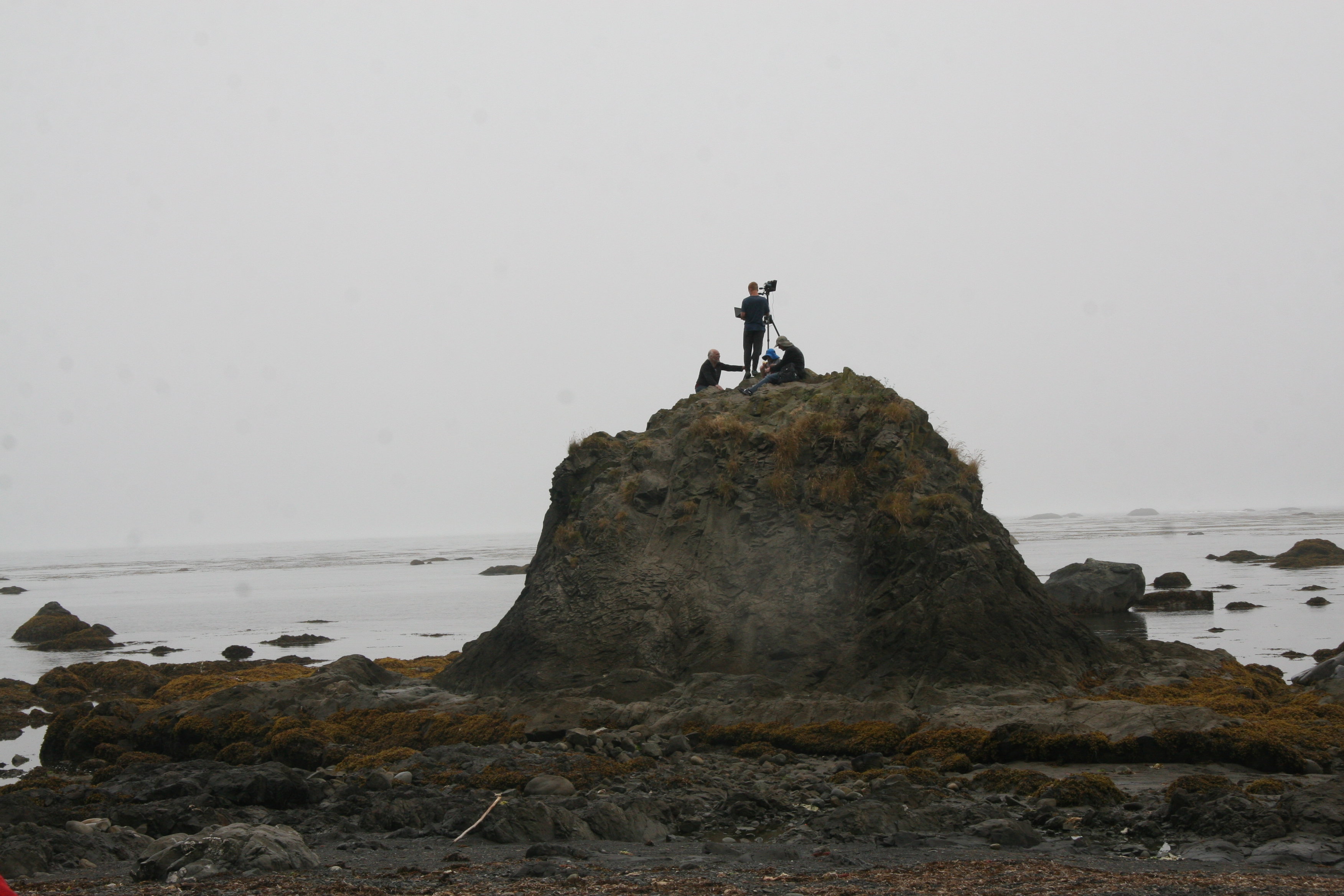
Setting 3D camera on the rock at Cape Alava
Testing 3D camera on a road tripIn August of 2017, my family and I went on a trip to the Pacific Northwest, partially for a much needed vacation, but equally as importantly, to test my dad’s new 3D camera. My dad had been designing calibrated multi-sensor cameras for as long as I can remember, and since February was working determinately on developing principally new algorithms for reconstructing a 3D model from a set of 4 simultaneously taken photographs . Now that the camera and the software were ready, there was no better time to test it.
The main portion of our trip was spent at the Olympic Peninsula in Washington. The gorgeous and complex natural setting was perfect for testing the abilities and limits of the camera. The camera lenses are arranged in a square configuration, each lens the same distance apart from the other. Such configuration is mimicking the position of human eyes, while adding the vertical pair helps measure distances to horizontal objects as well as vertical ones. Our depth perception, comes entirely from our brain’s ability to combine together two (from each eye) images to create a 3D space within our mind. The camera operates very similarly, using parallax, the technique that has been used throughout time to calculate distances using fairly simple geometry. Elphel 3D camera takes four individual images, which is more precise than two, and our software program calculates the distances to each object in the scene, combining data from 4 photographs and creates 3D model of the scene. You can explore our models with Elphel 3D model viewer: https://community.elphel.com/3d+map Also the models can be opened with 3D modeling program, such as Blender, and as a result you appear to be standing in a 3D realm, experiencing the environment, in a whole new sense .
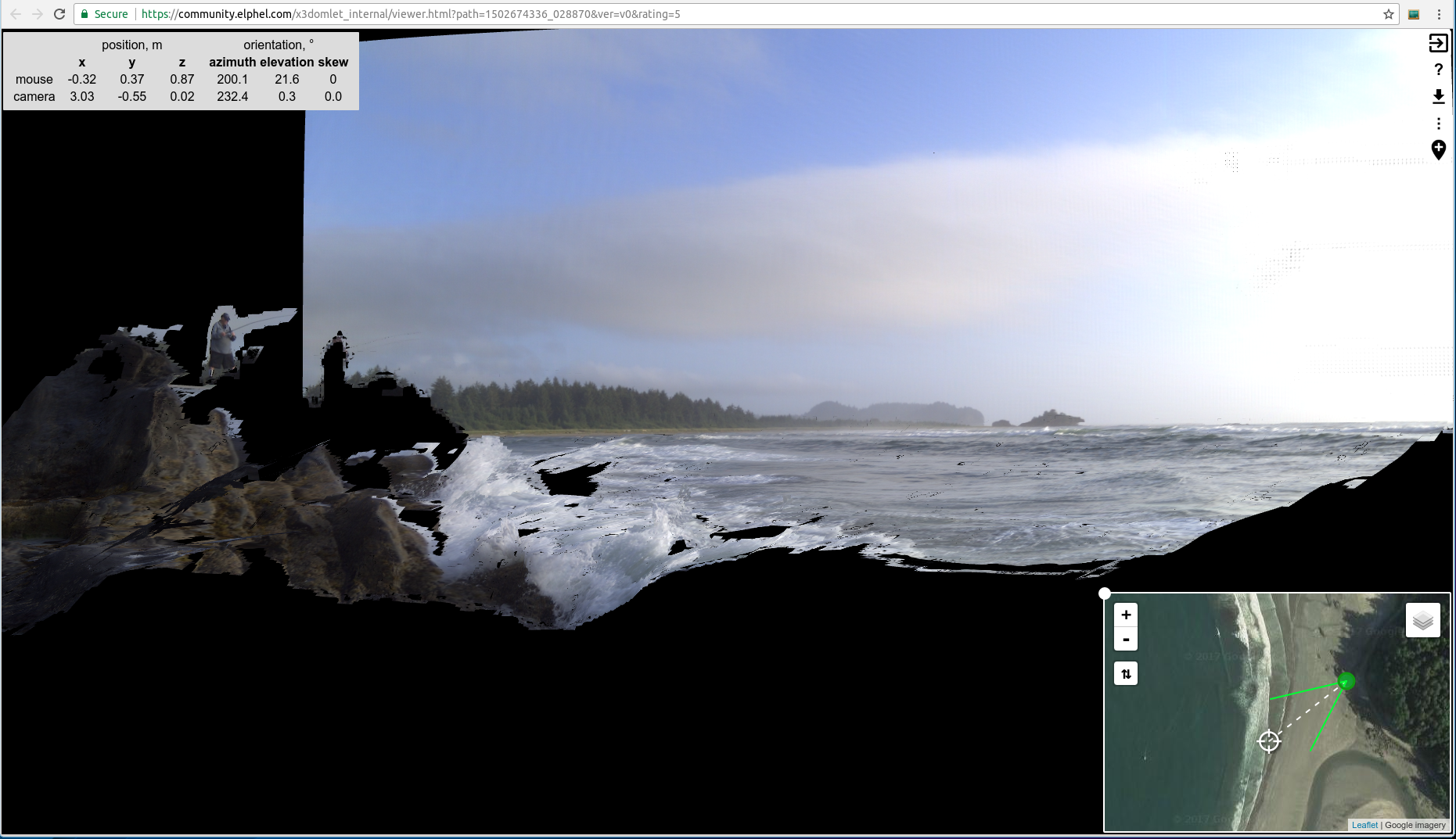
screenshot of the 3D model of ocean waves
Although the camera is meant to be a long-range photogrammetric camera, capable of accurately measuring distances at 200 meters and farther, we were fascinated with the idea of creating realistic 3D environments where we can virtually walk through. Throughout most of the testing we chose locations which would include the complex organic forms of nature, as to test the camera’s ability to work with finer details and non-geometric forms . Naturally, we shot parts of the Olympic National Park rain forest, with very exciting results. We also photographed the ocean waves crashing onto the shores rocks, and many more natural beauties. While my brother and I were taking the photographs, many times we would have to scale rocks, laptop and tripod in hand, in order to get the proper location. The process could get tedious, but at times was oddly exciting. At one point, we wanted to get an up-close shot of the waves just as they were arching over the rocks, but to do so, I had to act as a shield in case the water got too close to the camera, ready to leap in front of it at any time. Another time, my brother packed the camera into his backpack and biked to the most northwestern point on the US mainland, Cape Flattery, and took a series of images there. My dad had also used the images we had taken as the test data to find and fix bugs in his software.
All in all, the experience was really helpful, the vacation was rejuvenating, and the results were astounding, and it gave me the feeling that my family and I were creating something of the future. I don’t really know how this whole idea wouldn’t be considered exciting. Imagine, if you could just take a picture, and have it turned into a 3D space. Not only does the idea itself seem like the fantastic inventions of any quality science fiction (aka super cool), but it’s application to the real world are endless.
Working with Elphel models in BlenderWe have selected our favorite scenes to create a virtual path through the Olympic rain forest. Each model can be generated with a specified level of details, usually 500 meshes is enough for many scenes, however the rain forest looks more realistic when it is created with 2000 meshes.
$("#forest01").player(1); Tutorial
The procedure for importing and combining 3D model files in Blender, a Free software for 3D modeling and animation, is fairly simple.
Elphel example 3D meshes can be downloaded from https://community.elphel.com/3d+map by opening the desired scene, pressing the download icon (↓) and extracting archive into directory on your computer.
3D scene download
Download Blender form this link: https://www.blender.org/download/, and follow the installation instructions available for Linux, Windows, and Mac.
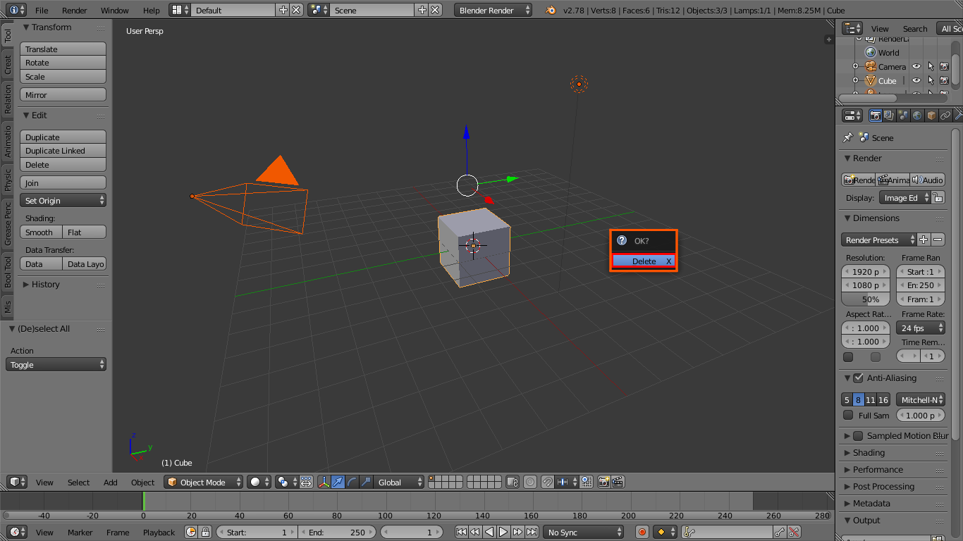
Once Blender has been opened, the scene must be cleared. This is done by pressing “a” until everything is highlighted and then pressing “x”
Clear scene
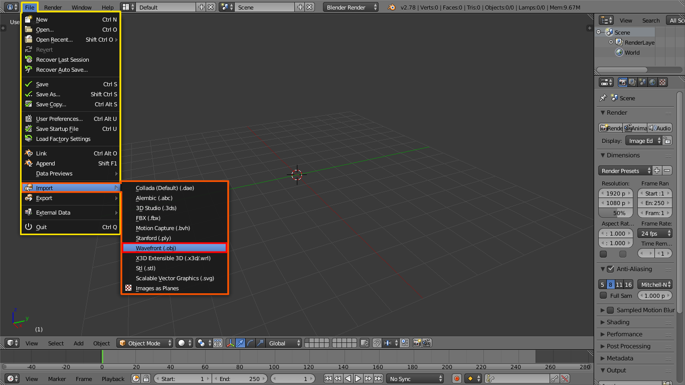
The 3D model file can then be opened in Blender by selecting the .obj option in the import menu and then selecting the downloaded *.obj file.
Import menu in Blender
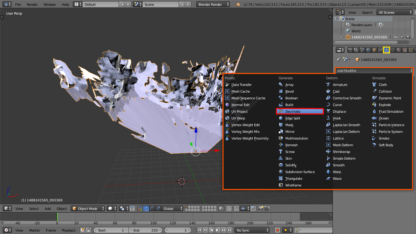
Follow these instructions if the computer struggles with graphics:
On right side of the window you will find the modifier options on the properties panel. Select the decimate modifier and set a ratio that works for your computer, this ratio will reduce the number of triangles but might also seriously warp textures. Do not press the apply button as viewport performance has already been improved.
Decimate modifier reduces the number of triangles
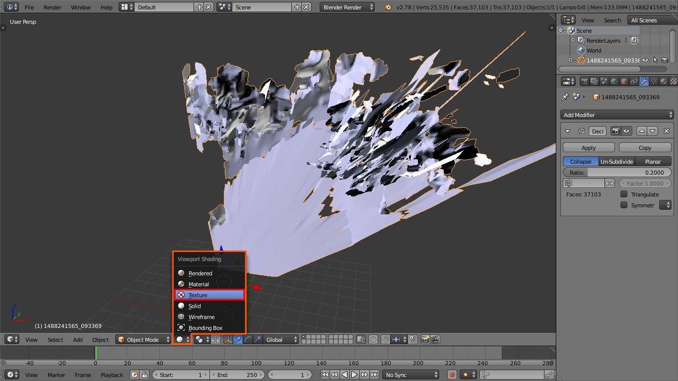
You will find that the imported mesh is gray; to view the textures change the viewport render mode to textured at the bottom of the 3d viewport (this may take a while on slower computers).
Texture mode
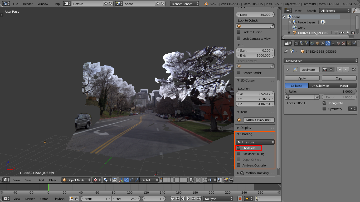
Now that textures are enabled, simulated lighting must be disabled. To do this hover mouse over the viewport and press “n” to open the properties region. Under the display tab check the “shadeless” box (this option is only available if the viewport render mode is set to textured).
Imported mesh with textures
The procedure can be repeated to import more models and manipulate them in Blender creating panoramic view of the city streets, path in the forest and other realistic 3D environments.
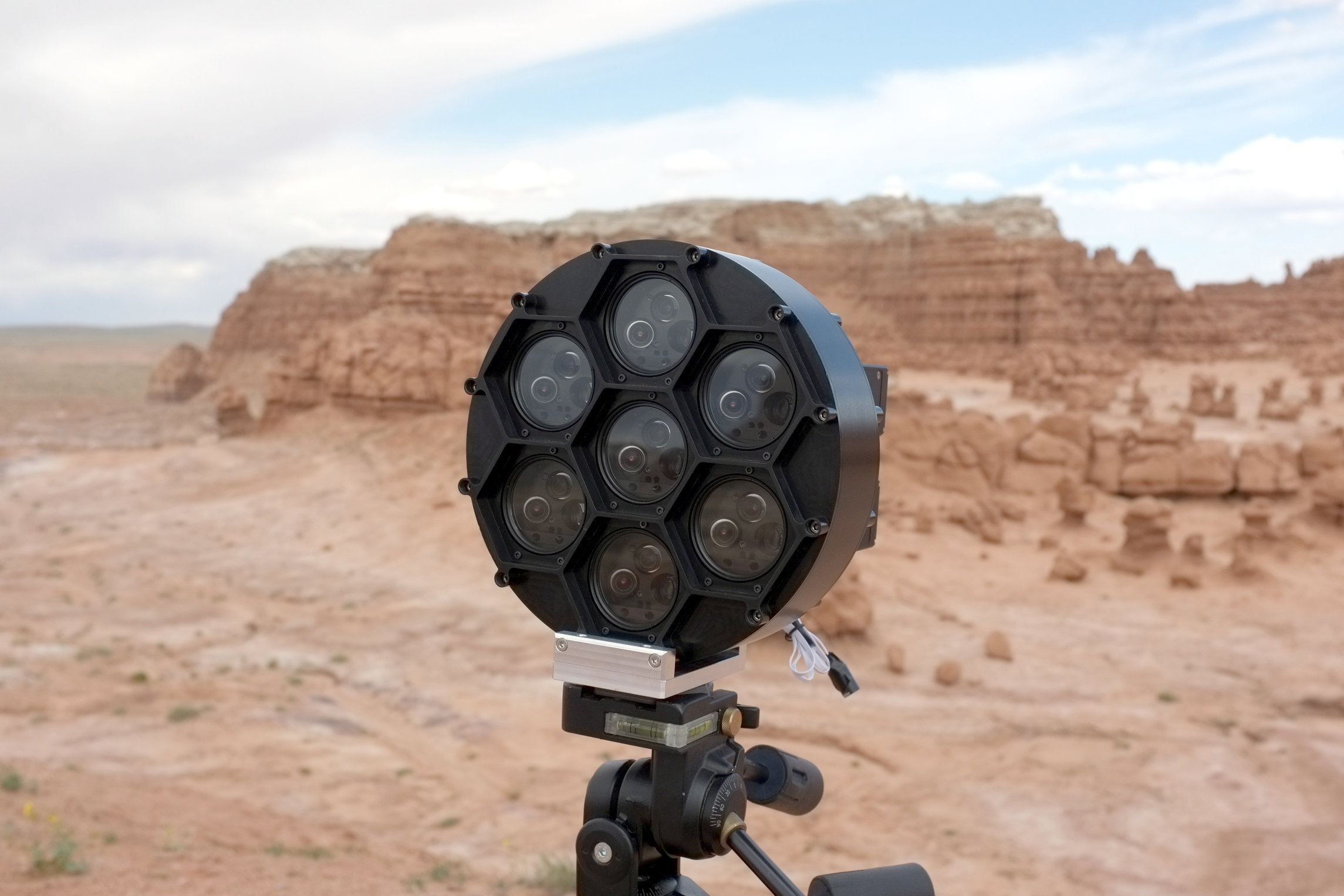
Long range multi-view stereo camera with 4 sensors
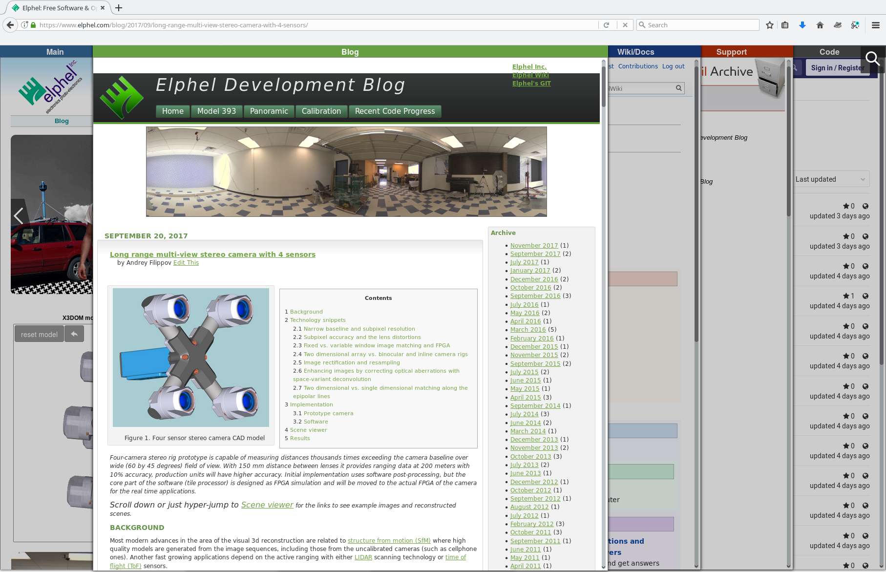
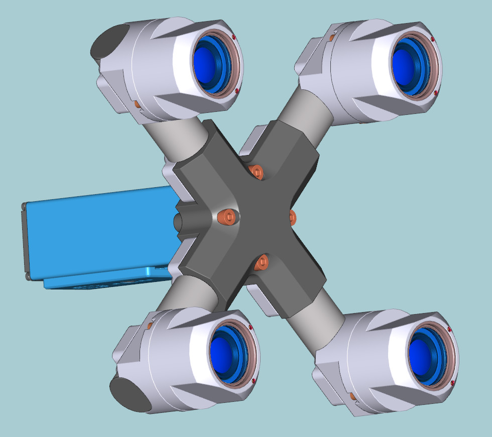
Figure 1. Four sensor stereo camera model
Four-camera stereo rig prototype is capable of measuring distances thousands times exceeding the camera baseline over wide (60 by 45 degrees) field of view. With 150 mm distance between lenses it provides ranging data at 200 meters with 10% accuracy, production units will have higher accuracy. Initial implementation uses software post-processing, but the core part of the software (tile processor) is designed as FPGA simulation and will be moved to the actual FPGA of the camera for the real time applications.
Scroll down or just hyper-jump to Scene viewer for the links to see example images and reconstructed scenes.
BackgroundMost modern advances in the area of the visual 3d reconstruction are related to structure from motion (SfM) where high quality models are generated from the image sequences, including those from the uncalibrated cameras (such as cellphone ones). Another fast growing applications depend on the active ranging with either LIDAR scanning technology or time of flight (ToF) sensors.
Each of these methods has its limitations and while widespread smart phone cameras attracted most of the interest in the algorithms and software development, there are some applications where the narrow baseline (distance between the sensors is much smaller, than the distance to the objects) technology has advantages.
Such applications include autonomous vehicle navigation where other objects in the scene are moving and 3-d data is needed immediately (not when the complete image sequence is captured), and the elements to be ranged are ahead of the vehicle so previous images would not help much. ToF sensors are still very limited in range (few meters) and the scanning LIDAR systems are either slow to update or have very limited field of view. Passive (visual only) ranging may be desired for military applications where the system should stay invisible by not shining lasers around.
Technology snippets Narrow baseline and subpixel resolutionThe main challenge for the narrow baseline systems is that the distance resolution is much worse than the lateral one. The minimal resolved 3d element, voxel is very far from resembling a cube (as 2d pixels are usually squares) – with the dimensions we use: pixel size – 0.0022 mm, lens focal length f = 4.5 mm and the baseline of 150 mm such voxel at 100 m distance is 50 mm high by 50 mm wide and 32 meters deep. The good thing is that while the lateral resolution generally is just one pixel (can be better only with additional knowledge about the object), the depth resolution can be improved with reasonable assumptions by an order of magnitude by using subpixel resolution. It is possible when there are multiple shifted images of the same object (that for such high range to baseline ratio can safely be assumed fronto-parallel) and every object is presented in each image by multiple pixels. With 0.1 pixel resolution in disparity (or shift between the two images) the depth dimension of the voxel at 100 m distance is 3.2 meters. And as we need multiple pixel objects for the subpixel disparity resolution, the voxel lateral dimensions increase (there is a way to restore the lateral resolution to a single pixel in most cases). With fixed-width window for the image matching we use 8×8 pixel grid (16×16 pixel overlapping tiles) similar to what is used by some image/video compression algorithms (such as JPEG) the voxel dimensions at 100 meter range become 0.4 m x 0.4 m x 3.2 m. Still not a cube, but the difference is significantly less dramatic.
Subpixel accuracy and the lens distortionsMatching images with subpixel accuracy requires that lens optical distortion of each lens is known and compensated with the same or better precision. Most popular way to present lens distortions is to use radial distortion model where relation of distorted and ideal pin-hole camera image is expressed as polynomial of point radius, so in polar coordinates the angle stays the same while the radius changes. Fisheye lenses are better described with “f-theta” model, where linear radial distance in the focal plane corresponds to the angle between the lens axis and ray to the object.
Such radial models provide accurate results only with ideal lens elements and when such elements are assembled so that the axis of each individual lens element precisely matches axes of the other elements – both in position and orientation. In the real lenses each optical element has minor misalignment, and that limits the radial model. For the lenses we had dealt with and with 5MPix sensors it was possible to get down to 0.2 – 0.3 pixels, so we supplemented the radial distortion described by the analytical formula with the table-based residual image correction. Such correction reduced the minimal resolved disparity to 0.05 – 0.08 pixels.
Fixed vs. variable window image matching and FPGAModern multi-view stereo systems that work with wide baselines use elaborate algorithms with variable size windows when matching image pairs, down to single pixels. They aggregate data from the neighbor pixels at later processing stages, that allows them to handle occlusions and perspective distortions that make paired images different. With the narrow baseline system, ranging objects at distances that are hundreds to thousands times larger than the baseline, the difference in perspective distortions of the images is almost always very small. And as the only way to get subpixel resolution requires matching of many pixels at once anyway, use of the fixed size image tiles instead of the individual pixels does not reduce flexibility of the algorithm much.
Processing of the fixed-size image tiles promises significant advantage – hardware-accelerated pixel-level tile processing combined with the higher level software that operates with the per-tile data rather than with per-pixel one. Tile processing can be implemented within the FPGA-friendly stream processing paradigm leaving decision making to the software. Matching image tiles may be implemented using methods similar to those used for image and especially video compression where motion vector estimation is similar to calculation of the disparity between the stereo images and similar algorithms may be used, such as phase-only correlation (PoC).
Two dimensional array vs. binocular and inline camera rigsUsually stereo cameras or fixed baseline multi-view stereo are binocular systems, with just two sensors. Less common systems have more than two lenses positioned along the same line. Such configurations improve the useful camera range (ability to measure near and far objects) and reduce ambiguity when dealing with periodic object structures. Even less common are the rigs where the individual cameras form a 2d structure.
In this project we used a camera with 4 sensors located in the corners of a square, so they are not co-linear. Correlation-based matching of the images depends on the detailed texture in the matched areas of the images – perfectly uniform objects produce no data for depth estimation. Additionally some common types of image details may be unsuitable for certain orientations of the camera baselines. Vertical concrete pole can be easily correlated by the two horizontally positioned cameras, but if the baseline is turned vertical, the same binocular camera rig would fail to produce disparity value. Similar is true when trying to capture horizontal features with the horizontal binocular system – such predominantly horizontal features are common when viewing near flat horizontal surfaces at high angles of incidents (almost parallel to the view direction).
With four cameras we process four image pairs – 2 horizontal (top and bottom) and 2 vertical (right and left), and depending on the application requirements for particular image region it is possible to combine correlation results of all 4 pairs, or just horizontal and vertical separately. When all 4 baselines have equal length it is easier to combine image data before calculating the precise location of the correlation maximums – 2 pairs can be combined directly, and the 2 others after rotating tiles by 90 degrees (swapping X and Y directions, transposing the tiles 2d arrays).
Image rectification and resamplingMany implementations of the multi-view stereo processing start with the image rectification that involves correction for the perspective and lens distortions, projection of the individual images to the common plane. Such projection simplifies image tiles matching by correlation, but as it involves resampling of the images, it either reduces resolution or requires upsampling and so increases required memory size and processing complexity.
This implementation does not require full de-warping of the images and related resampling with fractional pixel shifts. Instead we split geometric distortion of each lens into two parts:
- common (average) distortion of all four lenses approximated by analytical radial distortion model, and
- small residual deviation of each lens image transformation from the common distortion model
Common radial distortion parameters are used to calculate matching tile location in each image, and while integer rounded pixel shifts of the tile centers are used directly when selecting input pixel windows, the fractional pixel remainders are preserved and combined with the other image shifts in the FPGA tile processor. Matching of the images is performed in this common distorted space, the tile grid is also mapped to this presentation, not to the fully rectified rectilinear image.
Small individual lens deviations from the common distortion model are smooth 2-d functions over the 2-d image plane, they are interpolated from the calibration data stored for the lower resolution grid.
We use low distortion sorted lenses with matching focal lengths to make sure that the scale mismatch between the image tiles is less than tile size in the target subpixel intervals (0.1 pix). Low distortion requirement extends the distances range to the near objects, because with the higher disparity values matching tiles in the different images land to the differently distorted areas. Focal length matching allows to use modulated complex lapped transform (CLT) that similar to discrete Fourier transform (DFT) is invariant to shifts, but not to scaling (log-polar coordinates are not applicable here, as such transformation would deny shift invariance).
Enhancing images by correcting optical aberrations with space-variant deconvolutionMatching of the images acquired with the almost identical lenses is rather insensitive to the lens aberrations that degrade image quality (mostly reduce sharpness), especially in the peripheral image areas. Aberration correction is still needed to get sharp textures in the result 3d models over full field of view, the resolution of the modern sensors is usually better than what lenses can provide. Correction can be implemented with space-variant (different kernels for different areas of the image) deconvolution, we routinely use it for post-processing of Eyesis4π images. The DCT-based implementation is described in the earlier blog post.
Space-variant deconvolution kernels can absorb (be combined with during calibration processing) the individual lens deviations from the common distortion model, described above. Aberration correction and image rectification to the common image space can be performed simultaneously using the same processing resources.
Two dimensional vs. single dimensional matching along the epipolar linesCommon approach for matching image pairs is to replace the two-dimensional correlation with a single-dimensional task by correlating pixels along the epipolar lines that are just horizontal lines for horizontally built binocular systems with the parallel optical axes. Aggregation of the correlation maximums locations between the neighbor parallel lines of pixels is preformed in the image pixels domain after each line is processed separately.
For tile-based processing it is beneficial to perform a full 2-d correlation as the phase correlation is performed in the frequency domain, and after the pointwise multiplication during aberration correction the image tiles are already available in the 2d frequency domain. Two dimensional correlation implies aggregation of data from multiple scan lines, it can tolerate (and be used to correct) small lens misalignments, with appropriate filtering it can be used to detect (and match) linear features.
Implementation Prototype cameraExperimental camera looks similar to Elphel regular H-camera – we just incorporated different sensor front ends (3d CAD model) that are used in Eyesis4π and added adjustment screws to align optical axes of the lenses (heading and tilt) and orientations of the image sensors (roll). Sensors are 5 Mpix 1/2″ format On Semiconductor MT9P006, lenses – Evetar N125B04530W.
We selected lenses with the same focal length within 1%, and calibrated the camera using our standard camera rotation machine and the target pattern. As we do not yet have production adjustment equipment and software, the adjustment took several iterations: calibrating the camera and measuring extrinsic parameters of each sensor front end, then rotating each of the adjustment screws according to spreadsheet-calculated values, and then re-running the whole calibration process again. Finally the calibration results: radial distortion parameters, SFE extrinsic parameters, vignetting and deconvolution kernels were converted to the form suitable for run-time application (now – during post-processing of the captured images).
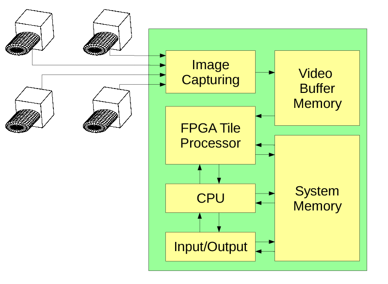
Figure 2. Camera block diagram
This prototype still uses 3d-printed parts and such mounts proved to be not stable enough, so we had to add field calibration and write code for bundle adjustment of the individual imagers orientations from the 2-d correlation data for each of the 4 individual pairs.
Camera performance depends on the actual mechanical stability, software-compensation can only partially mitigate this misalignment problem and the precision of the distance measurements was reduced when cameras went off by more than 20 pixels after being carried in a backpack. Nevertheless the scene reconstruction remained possible.
SoftwareMulti-view stereo rigs are capable of capturing dynamic scenes so our goal is to make a real-time system with most of the heavy-weight processing be done in the FPGA.
One of the major challenges here is how to combine parallel and stream processing capabilities of the FPGA with the flexibility of the software needed for implementation of the advanced 3d reconstruction algorithms. This approach is to use the FPGA-based tile processor to perform uniform operations on the lists of “tiles” – fixed square overlapping windows in the images. FPGA processes tile data at the pixel level, while software operates the whole tiles.
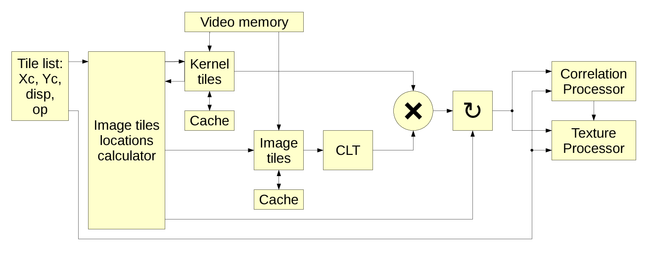
Figure 2 shows the overall block diagram of the camera, Figure 3 illustrates details of the tile processor.
Figure 3. FPGA tile processor
Initial implementation does not contain actual FPGA processing, so far we only tested in FPGA some of the core functions – two dimensional 8×8 DCT-IV needed for both 16×16 CLT and ICLT. Current code consists of the two separate parts – one part (tile processor) simulates what will be moved to the FPGA (it handles image tiles at the pixel level), and the other one is what will remain software – it operates on the tile level and does not deal with the individual pixels. These two parts interact using shared system memory, tile processor has exclusive access to the dedicated image buffer and calibration data.
Each tile is 16×16 pixels square with 8 pixel overlap, software prepares tile list including:
- tile center X,Y (for the virtual “center” image),
- center disparity, so the each of the 4 image tiles will be shifted accordingly, and
- the code of operation(s) to be performed on that tile.
Figure 4. Correlation processor
Tile processor performs all or some (depending on the tile operation codes) of the following operations:
- Reads the tile tasks from the shared system memory.
- Calculates locations and loads image and calibration data from the external image buffer memory (using on-chip memory to cache data as the overlapping nature of the tiles makes each pixel to participate on average in 4 neighbor tiles).
- Converts tiles to frequency domain using CLT based on 2d DCT-IV and DST-IV.
- Performs aberration correction in the frequency domain by pointwise multiplication by the calibration kernels.
- Calculates correlation-related data (Figure 4) for the tile pairs, resulting in tile disparity and disparity confidence values for all pairs combined, and/or more specific correlation types by pointwise multiplication, inverse CLT to the pixel domain, filtering and local maximums extraction by quadratic interpolation or windowed center of mass calculation.
- Calculates combined texture for the tile (Figure 5), using alpha channel to mask out pixels that do not match – this is the way how to effectively restore single-pixel lateral resolution after aggregating individual pixels to tiles. Textures can be combined after only programmed shifts according to specified disparity, or use additional shift calculated in the correlation module.
- Calculates other integral values for the tiles (Figure 5), such as per-channel number of mismatched pixels – such data can be used for quick second-level (using tiles instead of pixels) correlation runs to determine which 3d volumes potentially have objects and so need regular (pixel-level) matching.
- Finally tile processor saves results: correlation values and/or texture tile to the shared system memory, so software can access this data.
Figure 5. Texture processor
Single tile processor operation deals with the scene objects that would be projected to this tile’s 16×16 pixels square on the sensor of the virtual camera located in the center between the four actual physical cameras. The single pass over the tile data is limited not just laterally, but in depth also because for the tiles to correlate they have to have significant overlap. 50% overlap corresponds to the correlation offset range of ±8 pixels, better correlation contrast needs 75% overlap or ±4 pixels. The tile processor “probes” not all the voxels that project to the same 16×16 window of the virtual image, but only those that belong to the certain distance range – the distances that correspond to the disparities ±4 pixels from the value provided for the tile.
That means that a single processing pass over a tile captures data in a disparity space volume, or a macro-voxel of 8 pixels wide by 8 pixels high by 8 pixels deep (considering the central part of the overlapping volumes). And capturing the whole scene may require multiple passes for the same tile with different disparity. There are ways how to avoid full range disparity sweep (with 8 pixel increments) for all tiles – following surfaces and detecting occlusions and discontinuities, second-level correlation of tiles instead of the individual pixels.
Another reason for the multi-pass processing of the same tile is to refine the disparity measured by correlation. When dealing with subpixel coordinates of the correlation maximums – either located by quadratic approximation or by some form of center of mass evaluation, the calculated values may have bias and disparity histograms reveal modulation with the pixel period. Second “refine” pass, where individual tiles are shifted by the disparity measured in the previous pass reduces the residual offset of the correlation maximum to a fraction of a pixel and mitigates this type of bias. Tile shift here means a combination of the integer pixel shift of the source images and the fractional (in the ±0.5 pixel range) shift that is performed in the frequency domain by multiplication by the cosine/sine phase rotator.
Total processing time and/or required FPGA resources linearly depend on the number of required tile processor operations and the software may use several methods to reduce this number. In addition to the two approaches mentioned above (following surfaces and second-level correlation) it may be possible to reduce the field of view to a smaller area of interest, predict current frame scene from the previous frames (as in 2d video compression) – tile processor paradigm preserves flexibility of the various algorithms that may be used in the scene 3d reconstruction software stack.
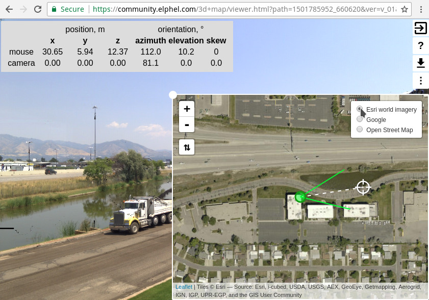
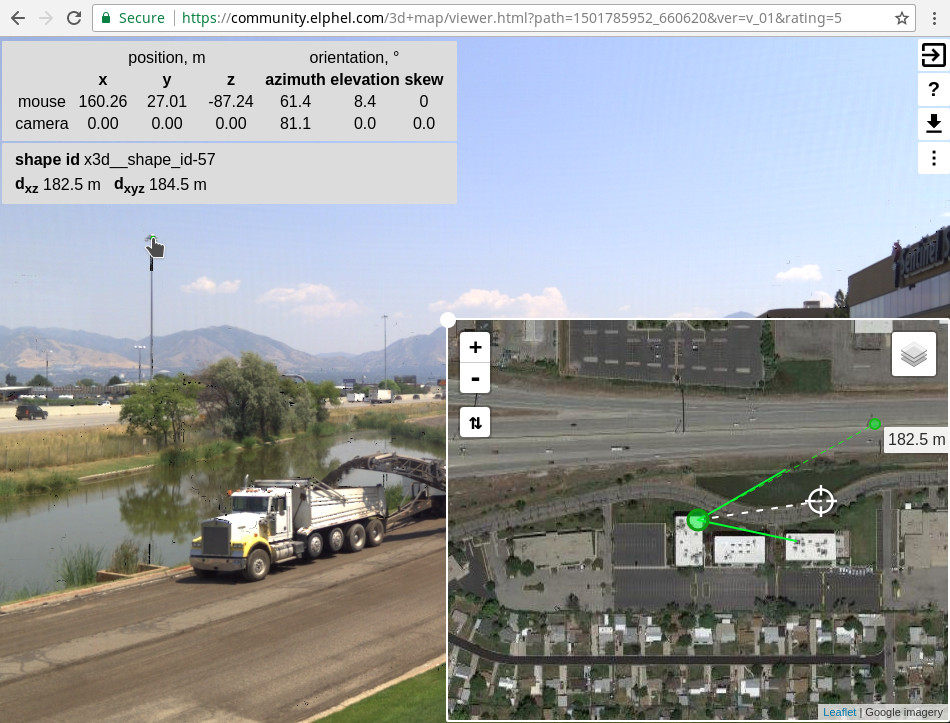
Scene viewerThe viewer for the reconstructed scenes is here: https://community.elphel.com/3d+map (viewer source code).
Figure 6. 3d+map index page
Index page shows a map (you may select from several providers) with the markers for the locations of the captured scenes. On the left there is a vertical ribbon of the thumbnails – you may scroll it with a mouse wheel or by dragging.
Thumbnails are shown only for the markers that fit on screen, so zooming in on the map may reduce number of the visible thumbnails. When you select some thumbnail, the corresponding marker opens on the map, and one or several scenes are shown – one line per each scene (identified by the Unix timestamp code with fractional seconds) captured at the same locations.
The scene that matches the selected thumbnail is highlighted (as 4-th line in the Figure 6). Some scenes have different versions of reconstruction from the same source images – they are listed in the same line (like first line in the Figure 6). Links lead to the viewers of the selected scene/version.
Figure 7. Selection of the map / satellite imagery provider
We do not have ground truth models for the captured scenes build with the active scanners. Instead as the most interesting is ranging of the distant objects (hundreds of meters) it is possible to use publicly available satellite imagery and match it to the captured models. We had ideal view from Elphel office window – each crack on the pavement was visible in the satellite images so we could match them with the 3d model of the scene. Unfortunately they ruined it recently by replacing asphalt :-).
The scene viewer combines x3dom representation of the 3d scene and the re-sizable overlapping map view. You may switch the map imagery provider by clicking on the map icon as shown in the Figure 7.
The scene and map views are synchronized to each other, there are several ways of navigation in either 3d or map area:
- drag the 3d view to rotate virtual camera without moving;
- move cross-hair ⌖ icon in the map view to rotate camera around vertical axis;
- toggle ⇅ button and adjust camera view elevation;
- use scroll wheel over the 3d area to change camera zoom (field of view is indicated on the map);
- drag with middle button pressed in the 3d view to move camera perpendicular to the view direction;
- drag the the camera icon (green circle) on the map to move camera horizontally;
- toggle ⇅ button and move the camera vertically;
- press a hotkey t over the 3d area to reset to the initial view: set azimuth and elevation same as captured;
- press a hotkey r over the 3d area to set view azimuth as captured, elevation equal to zero (horizontal view).
Figure 8. 3D model to map comparison
Comparison of the 3d scene model and the map uses ball markers. By default these markers are one meter in diameter, the size can be changed on the settings (⋮) page.
Moving pointer over the 3d area with Ctrl key pressed causes the ball to follow the cursor at a distance where the view line intersects the nearest detected surface in the scene. It simultaneously moves the corresponding marker over the map view and indicates the measured distance.
Ctrl-click places the ball marker on the 3d scene and on the map. It is then possible to drag the marker over the map and read the ground truth distance. Dragging the marker over the 3d scene updates location on the map, but not the other way around, in edit mode mismatch data is used to adjust the captured scene location and orientation.
Program settings used during reconstruction limit the scene far distance to z = 1000 meters, all more distant objects are considered to be located at infinity. X3d allows to use images at infinity using backdrop element, but it is not flexible enough and is not supported by some other programs. In most models we place infinity textures to a large billboard at z = 10,000 meters, and it is where the ball marker will appear if placed on the sky or other far objects.
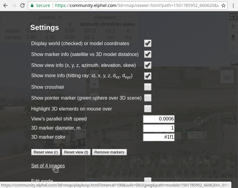
Figure 9. Settings and link to four images
The settings page (⋮) shown in the Figure 9 has a link to the four-image viewer (Figure 10). These four images correspond to the captured views and are almost “raw images” used for scene reconstruction. These images were subject to the optical aberration correction and are partially rectified – they are rendered as if they were captured by the same camera that has only strictly polynomial radial distortion.
Such images are not actually used in the reconstruction process, they are rendered only for the debug and demonstration purposes. The equivalent data exists in the tile processor only in the frequency domain form as an intermediate result, and was subject to just linear processing (to avoid possible unintended biases) so the images have some residual locally-checkerboard pattern that is due to the Bayer mosaic filter (discussed in the earlier blog). Textures that are generated from the combination of all four images have the contrast of such pattern significantly lower. It is possible to add some non-linear filtering at the very last stage of the texture generation.
Each scene model has a download link for the archive that contains the model itself as *.x3d file and Wavefront *.obj and *.mtl as well as the corresponding RGBA texture files as PNG images. Initially I missed the fact that x3d and obj formats have opposite direction of surface normals for the same triangular faces, so almost half of the Wavefront files still have incorrect (opposite direction) surface normals.
ResultsOur initial plan was to test algorithms for the tile processor before implementing them in FPGA. The tile processor provides data for the disparity space image (DSI) – confidence value of having certain disparity for specified 2d position in the image, it also generates texture tiles.
When the tile processor code was written and tested, we still needed some software to visualize the results. DSI itself seemed promising (much better coverage than what I had with earlier experiments with binocular images), but when I tried to convert these textured tiles into viewable x3d model directly, it was a big disappointment. Result did not look like a 3d scene – there were many narrow triangles that made sense only when viewed almost directly from the camera actual location, a small lateral viewpoint movement – and the image was falling apart into something unrecognizable.
Figure 10. Four channel images (click for actual viewer with zoom/pan capability)
I was not able to find ready to use code and the plan to write a quick demo for the tile processor and generated DSI seemed less and less realistic. Eventually it took at least three times longer to get somewhat usable output than to develop DCT-based tile processor code itself.
Current software is still incomplete, lacks many needed features (it even does not cut off background so wires over the sky steal a lot of surrounding space), it runs slow (several minutes per single scene), but it does provide a starting point to evaluate performance of the long range 4-camera multi-view stereo system. Much of the intended functionality does not work without more parameter tuning, but we decided to postpone improvements to the next stage (when we will have cameras that are more stable mechanically) and instead try to capture more of very different scenes, process them in batch mode (keeping the same parameter values for all new scenes) and see what will be the output.
As soon as the program was able to produce somewhat coherent 3d model from the very first image set captured through Elphel office window, Oleg Dzhimiev started development of the web application that allows to match the models with the map data. After adding more image sets I noticed that the camera calibration did not hold. Each individual sub-camera performed nicely (they use thermally compensated mechanical design), but their extrinsic parameters did change and we had to add code for field calibration that uses image themselves. The best accuracy in disparity measurement over the field of view still requires camera poses to match ones used at full calibration, so later scenes with more developed misalignment (>20 pixels) are less precise than earlier (captured in Salt Lake City).
We do not have an established method to measure ranging precision for different distances to object – the disparity values are calculated together with the confidence and in lower confidence areas the accuracy is lower, including places where no ranging is possible due to the complete absence of the visible details in the images. Instead it is possible to compare distances in various scene models to those on the map and see where such camera is useful. With 0.1 pixel disparity resolution and 150 mm baseline we should be able to measure 300 m distances with 10% accuracy, and for many captured scene objects it already is not much worse. We now placed orders to machine the new camera parts that are needed to build a more mechanically stable rig. And parallel to upgrading the hardware, we’ll start migrating the tile processor code from Java to Verilog.
And what’s next? Elphel goal is to provide our users with the high performance hackable products and freedom to modify them in the ways and for the purposes we could not imagine ourselves. But it is fun to fantasize about at least some possible applications:
- Obviously, self-driving cars – increased number of cameras located in a 2d pattern (square) results in significantly more robust matching even with low-contrast textures. It does not depend on sequential scanning and provides simultaneous data over wide field of view. Calculated confidence of distance measurements tells when alternative (active) ranging methods are needed – that would help to avoid infamous accident with a self-driving car that went under a truck.
- Visual odometry for the drones would also benefit from the higher robustness of image matching.
- Rovers on Mars or other planets using low-power passive (visual based) scene reconstruction.
- Maybe self-flying passenger multicopters in the heavy 3d traffic? Sure they will all be equipped with some transponders, but what about aerial roadkills? Like a flock of geese that forced water landing.
- High speed boating or sailing over uneven seas with active hydrofoils that can look ahead and adjust to the future waves.
- Landing on the asteroids for physical (not just Bitcoin) mining? With 150 mm baseline such camera can comfortably operate within several hundred meters from the object, with 1.5 m that will scale to kilometers.
- Cinematography: post-production depth of field control that would easily beat even the widest format optics, HDR with a pair of 4-sensor cameras, some new VFX?
- Multi-spectral imaging where more spatially separate cameras with different bandpass filters can be combined to the same texture in the 3d scene.
- Capturing underwater scenes and measuring how far the sea creatures are above the bottom.
- …
Current video stream latency and a way to reduce it
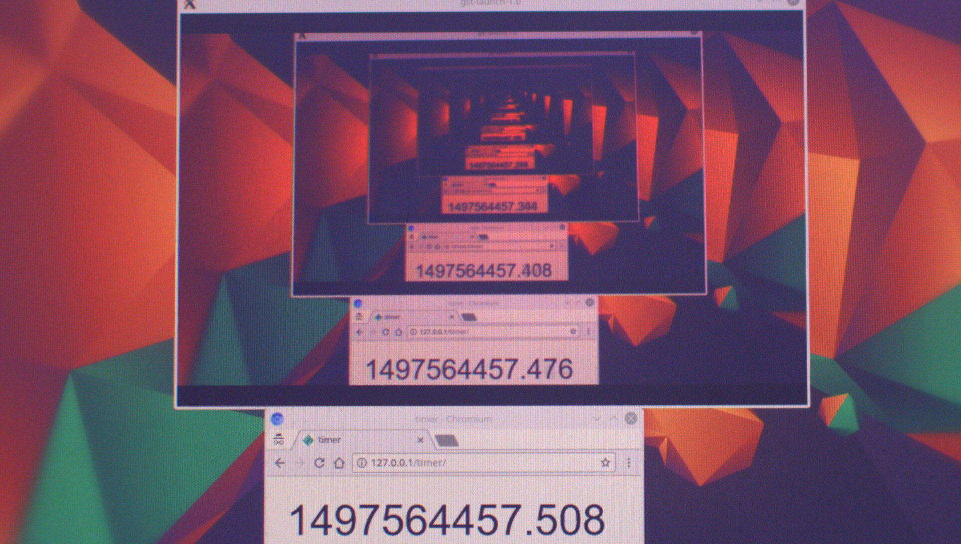
Fig.1 Live stream latency testing
Recently we had an inquiry whether our cameras are capable of streaming low latency video. The short answer is yes, the camera’s average output latency for 1080p at 30 fps is ~16 ms. It is possible to reduce it to almost 0.5 ms with a few changes to the driver.
However the total latency of the system, from capturing to displaying, includes delays caused by network, pc, software and display.
In the results of the experiment (similar to this one) these delays contribute the most (around 40-50 ms) to the stream latency – at least, for the given equipment.
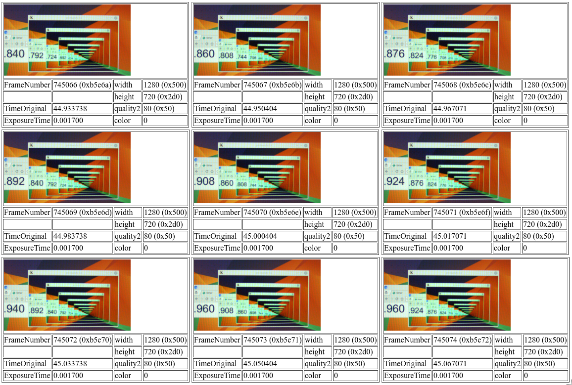
Measure the total latency of a live stream over network from 10393 camera.
- Camera: NC393-F-CS
- Resolution@fps: 1080p@30fps, 720p@60fps
- Compression quality: 90%
- Exposure time: 1.7 ms
- Stream formats: mjpeg, rtsp
- Sensor: MT9P001, 5MPx, 1/2.5″
- Lens: Computar f=5mm, f/1.4, 1/2″
- PC: Shuttle box, i7, 16GB RAM, GeForce GTX 560 Ti
- Display: ASUS VS24A, 60Hz (=16.7ms), 5ms gtg
- OS: Kubuntu 16.04
- Network connection: 1Gbps, direct camera-PC via cable
- Applications:
- gstreamer
- chrome, firefox
- mplayer
- vlc
- Stopwatch: basic javascript
Notes table{ border-collapse: collapse; } td{ padding:0px 5px; border:1px solid black; } th{ padding:5px; border:1px solid black; background:rgba(220,220,220,0.5); }
Fig.2 Image sensor is rotated 90°[/caption]
It's important to keep in mind that displays are refreshed progressively - so, if an image sensor is a rolling shutter type - their scan directions will coinside.
-->
Table 1: Transfer times and data rate
1 – average compressed (90%) image size
2 – time it takes to transfer a single image over network. Jitter is unknown. t = Image_size*1Gbps
3 – required bandwidth: rate = fps*Image_size
All numbers are for the given lens, sensor and camera setup and parameters. Briefly.
Sensor
Because of ERS each row’s latency is different. See tables 2 and 3.
Table 2: tROW and tTR
1 – row time, see datasheet. tROW = f(Width)
2 – time it takes to transfer a row over sensor cable, clock = 96MHz. tTR = Width/96MHz
Table 3: Average latency and the whole range.
1 – average latency
2 – min – last row latency, max – 1st row latency
Exposure
tEXP < 1 ms – typical exposure time for outdoors. A display is bright enough to set 1.7 ms with the gains maxed.
Compressor
The compressor is implemented in fpga and works 3x times faster but needs a stripe of 20 rows in memory. Thus, the compressor will finish ~20/3*tROW after the whole image is read out.
tCMP = 20/3*tROW
Summary
tCAM = tERS + tEXP + tCMP
Since the image is read and compressed by fpga logic of the Zynq and this pipeline has been simulated we can be sure in these numbers.
Table 4: Average output latency + exposure
Not accurate. For simplicity, we will rely on the camera’s internal clock that time stamps every image, and take the javascript timer readings as unique labels, thus not caring what time they are showing.
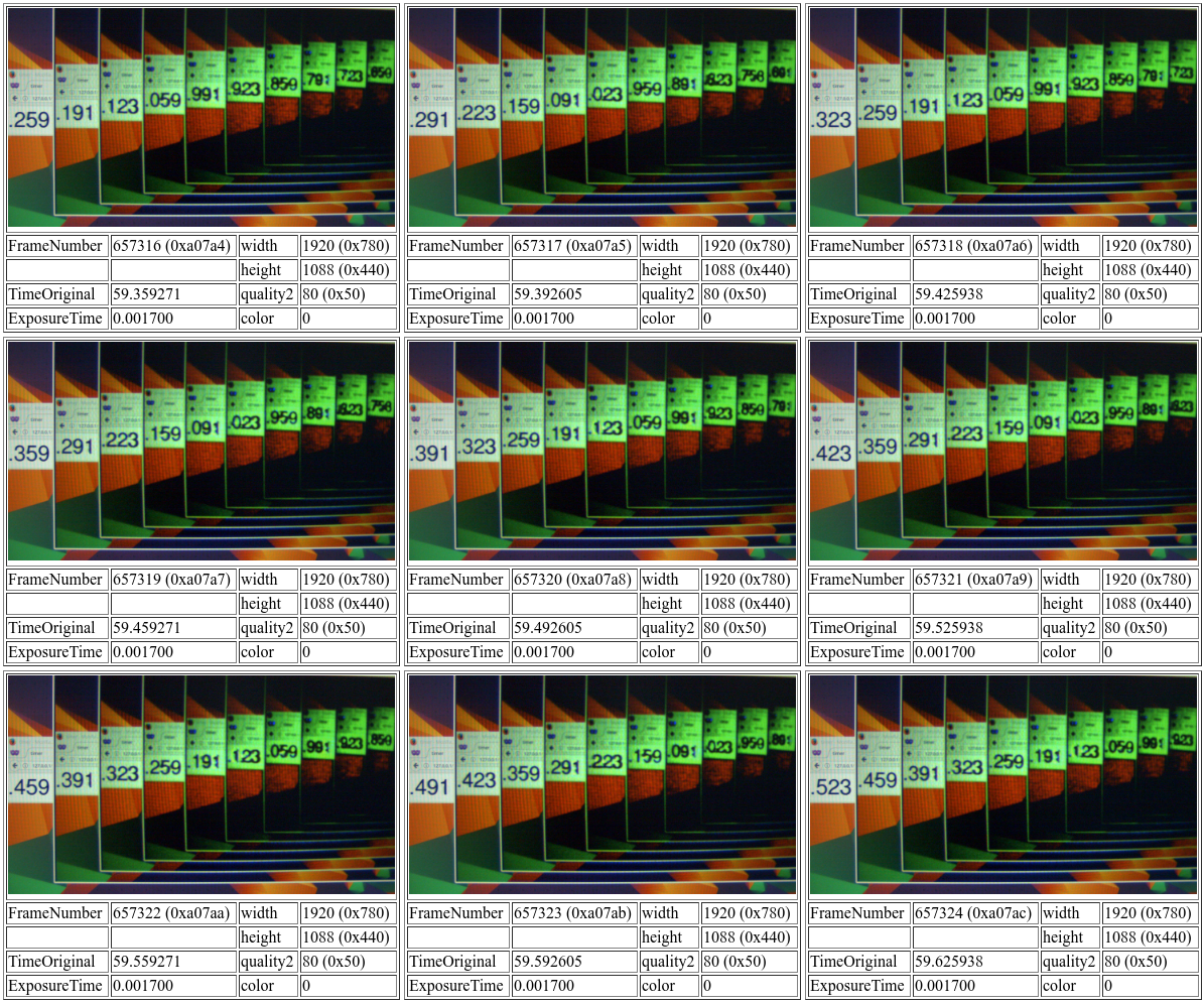
Fig.2 1080p 30fps
Fig.3 720p 60fps
GStreamer has shown the best results among the tested programs.
Since the camera fps is discrete the result is a multiple of 1/fps (see this article):
- 30 fps => 33.3 ms
- 60 fps => 16.7 ms
Resolution/fps Total Latency, ms Network+PC+SW latency, ms 720p@60fps 33.3-50 23.4-40.1 1080p@30fps 33.3-66.7 15.4-48.8
Possible improvements Camera
Currently, the driver waits for the interrupt from the compressor that indicates the image is fully compressed and ready for transfer. Meanwhile one does not have to wait for the whole image but start the transfer when the minimum of the compressed is data ready.
There are 3 more interrupts related to the image pipeline events. One of them is “compression started” – switching to it can reduce the output latency to (10+20/3)*tROW or 0.4 ms for 720p and 0.5 ms for 1080p.
Other hardware and softwareIn addition to the most obvious improvements:
- For wifi: use 5GHz over 2.4GHz – smaller jitter, non-overlapping channels
- Lower latency software: for mjpeg use gstreamer or vlc (takes an extra effort to setup) over chrome or firefox because they do extra buffering
- Latency in live network video surveillance
- Wifi latencies, 2.4GHz & 5GHz
- This video compares different displays.
- About ERS
Lapped MDCT-based image conditioning with optical aberrations correction, color conversion, edge emphasis and noise reduction
jQuery(window).load(function(){
jQuery("#sravnitel_0").sravnitel({
images: ["http://blog.elphel.com/wp-content/uploads/2017/01/1481779723_364497-00-raw-debayer-only-annotated.jpeg","http://blog.elphel.com/wp-content/uploads/2017/01/1481779723_364497-00-raw-debayer-only.jpeg","http://blog.elphel.com/wp-content/uploads/2017/01/1481779723_364497-00-no-color-processing-rgb-lpf.jpeg","http://blog.elphel.com/wp-content/uploads/2017/01/1481779723_364497-00-no-nonlin.jpeg","http://blog.elphel.com/wp-content/uploads/2017/01/1481779723_364497-00-no-denoise.jpeg","http://blog.elphel.com/wp-content/uploads/2017/01/1481779723_364497-00-processed.jpeg"],
titles: ["Raw image, standard bilinear 3x3 pixels kernel de-mosaic, annotated","Raw image, standard bilinear 3x3 pixels kernel de-mosaic","No color conversion, low pass filtered RGB only","Colors converted and low-pass filtered, no nonlinear processing","Edge emphasis enabled, no noise suppression","Fully processed with noise suppression"],
showtitles: true,
width: 750,
height: 560,
index_l: 0,
index_r: 5,
zoom: 1,
center_x: 1800,
center_y: 1150,
});
});
Fig.1. Image comparison of the different processing stages output
Results of the processing of the color image
Previous blog post “Lens aberration correction with the lapped MDCT” described our experiments with the lapped MDCT[1] for optical aberration corrections of a single color channel and separation of the asymmetrical kernel into a small asymmetrical part for direct convolution and a larger symmetrical one to be applied in the frequency domain of the MDCT. We supplemented this processing chain with additional steps of the image conditioning to evaluate the overall quality of the of the results and feasibility of the MDCT approach for processing in the camera FPGA.
Image comparator in Fig.1 allows to see the difference between the images generated from the results of the several stages of the processing. It makes possible to compare any two of the image layers by either sliding the image separator or by just clicking on the image – that alternates right/left images. Zoom is controlled by the scroll wheel (click on the zoom indicator fits image), pan – by dragging.
Original image was acquired with Elphel model 393 camera with 5 Mpix MT9P006 image sensor and Sunex DSL227 fisheye lens, saved in jp4 format as a raw Bayer data at 98% compression quality. Calibration was performed with the Java program using calibration pattern visible in the image itself. The program is designed to work with the low-distortion lenses so fisheye was a stretch and the calibration kernels near the edges are just replicated from the ones closer to the center, so aberration correction is only partial in those areas.
First two layers differ just by added annotations, they both show output of a simple bilinear demosaic processing, same as generated by the camera when running in JPEG mode. Next layers show different stages of the processing, details are provided later in this blog post.
Correction of the optical aberrations in the image can be viewed as convolution of the raw image array with the space-variant kernels derived from the optical point spread functions (PSF). In the general case of the true space-variant kernels (different for each pixel) it is not possible to use DFT-based convolution, but when the kernels change slowly and the image tiles can be considered isoplanatic (areas where PSF remains the same to the specified precision) it is possible to apply the same kernel to the whole image tile that is processed with DFT (or combined convolution/MDCT in our case). Such approach is studied in deep for astronomy [2],[3] (where they almost always have plenty of δ-function light sources to measure PSF in the field of view :-)).
The procedure described below is a combination of the sparse kernel convolution in the space domain with the lapped MDCT processing making use of its perfect (only approximate with the variant kernels) reconstruction property, but it still implements the same convolution with the variant kernels.
Signal flow is presented in Fig.2. Input signal is the raw image data from the sensor sampled through the color filter array organized as a standard Bayer mosaic: each 2×2 pixel tile includes one of the red and blue samples, and 2 of the green ones.
In addition to the image data the process depends on the calibration data – pairs of asymmetrical and symmetrical kernels calculated during camera calibration as described in the previous blog post.
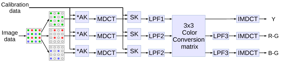
Fig.2. Signal flow of the linear part of MDCT-based image conditioning
Image data is processed in the following sequence of the linear operations, resulting in intensity (Y) and two color difference components:
- Input composite signal is split by colors into 3 separate channels producing sparse data in each.
- Each channel data is directly convolved with a small (we used just four non-zero elements) asymmetrical kernel AK, resulting in a sequence of 16×16 pixel tiles, overlapping by 8 pixels (input pixels are not limited to 16×16 tiles).
- Each tile is multiplied by a window function, folded and converted with 8×8 pixel DCT-IV[4] – equivalent of the 16×16->8×8 MDCT.
- 8×8 result tiles are multiplied by symmetrical kernels (SK) – equivalent of convolving the pre-MDCT signal.
- Each channel is subject to the low-pass filter that is implemented by multiplying in the frequency domain as these filters are indeed symmetrical. The cutoff frequency is different for the green (LPF1) and other (LPF2) colors as there are more source samples for the first. That was the last step before inverse transformation presented in the previous blog post, now we continued with a few more.
- Natural images have strong correlation between different color channels so most image processing (and compression) algorithms involve converting the pure color channels into intensity (Y) and two color difference signals that have lower bandwidth than intensity. There are different standards for the color conversion coefficients and here we are free to use any as this process is not a part of a matched encoder/decoder pair. All such conversions can be represented as a 3×3 matrix multiplication by the (r,g,b) vector.
- Two of the output signals – color differences are subject to an additional bandwidth limiting by LPF3.
- IMDCT includes 8×8 DCT-IV, unfolding 8×8 into 16×16 tiles, second multiplication by the window function and accumulation of the overlapping tiles in the pixel domain.
For some applications the output data is already useful – ideally it has all the optical aberrations compensated so the remaining far-reaching inter-pixel correlation caused by a camera system is removed. Next steps (such as stereo matching) can be done on- (or off-) line, and the algorithms do not have to deal with the lens specifics. Other applications may benefit from additional processing that improves image quality – at least the perceived one.
Such processing may target the following goals:
- To reduce remaining signal modulation caused by the Bayer pattern (each source pixel carries data about a single color component, not all 3), trying to remove it by a LPF would blur the image itself.
- Detect and enhance edges, as most useful high-frequency elements represent locally linear features
- Reduce visible noise in the uniform areas (such as blue sky) where significant (especially for the small-pixel sensors) noise originates from the shot noise of the pixels. This noise is amplified by the aberration correction that effectively increases the high frequency gain of the system.
Some of these three goals overlap and can be addressed simultaneously – edge detection can improve de-mosaic quality and reduce related colored artifacts on the sharp edges if the signal is blurred along the edges and simultaneously sharpened in the orthogonal direction. Areas that do not have pronounced linear features are likely to be uniform and so can be low-pass filtered.
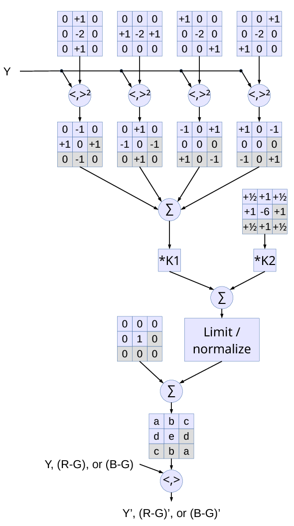
The non-linear processing produces modified pixel value using 3×3 pixel array centered around the current pixel. This is a two-step process:
- First the 3×3 center-symmetric matrices (one for Y, another for color) of coefficients are calculated using the Y channel data, then
- they are applied to the Y and color components by replacing the pixel value with the inner product of the calculated coefficients and the original data.
Signal flow for one channel is presented in Fig.3:
Fig.3 Non-linear image processing: edge emphasis and noise reduction
- Four inner products are calculated for the same 9-sample Y data and the shown matrices (corresponding to second derivatives along vertical, horizontal and the two diagonal directions).
- Each of these values is squared and
- the following four 3×3 matrices are multiplied by these values. Matrices are symmetrical around the center, so gray-colored cells do not need to be calculated.
- Four matrices are then added together and scaled by a variable parameter K1. The first two matrices are opposite to each other, and so are the second two. So if the absolute value of the two orthogonal second derivatives are equal (no linear features detected), the corresponding matrices will annihilate each other.
- A separate 3×3 matrix representing a weighted running average, scaled by K2 is added for noise reduction.
- The sum of the positive values is compared to a specified threshold value, and if it exceed it – all the matrix is proportionally scaled down – that makes different line directions to “compete” against each other and against the blurring kernel.
- The sum of all 9 elements of the calculated array is zero, so the default unity kernel is added and when correction coefficients are zeros, the result pixels will be the same as the input ones.
- Inner product of the calculated 9-element array and the input data is calculated and used as a new pixel value. Two of the arrays are created from the same Y channel data – one for Y and the other for two color differences, configurable parameters (K1, K2, threshold and the smoothing matrix) are independent in these two cases.
The described method of the optical aberration correction is tested with the software implementation that uses only operations that can be ported to the FPGA, so we are almost ready to get back to to Verilog programming. One more thing to try before is to see if it is possible to merge this correction with a minor distortion correction. DFT and DCT transforms are not good at scaling the images (when using the same pixel grid). It is definitely not possible no rectify large areas of the fisheye images, but maybe small (fraction of a pixel per tile) stretching can still be absorbed in the same step with shifting? This may have several implications.
Single-step image rectificationIt would be definitely attractive to eliminate additional processing step and save FPGA resources and/or decrease the processing time. But there is more than that – re-sampling degrades image resolution. For that reason we use half-pixel grid for the offline processing, but it increases amount of data 4 times and processing resources – at least 4 times also.
When working with the whole pixel grid (as we plan to implement in the camera FPGA) we already deal with the partial pixel shifts during convolution for aberration correction, so it would be very attractive to combine these two fractional pixel shifts into one (calibration process uses half-pixel grid) and so to avoid double re-sampling and related image degrading.
Using analytical lens distortion model with the precision of the pixel mappingAnother goal that seems achievable is to absorb at least the table-based pixel mapping. Real lenses can only to some precision be described by an analytical formula of a radial distortion model. Each element can have errors and the multi-lens assembly can inevitably has some mis-alignments – all that makes the lenses different and deviate from a perfect symmetry of the radial model. When we were working with (rather low distortion) wide angle lenses Evetar N125B04530W we were able to get to 0.2-0.3 pix root mean square of the reprojection error in a 26-lens camera system when using radial distortion model with up to the 8-th power of the radial polynomial (insignificant improvement when going from 6-th to the 8-th power). That error was reduced to 0.05..0.07 pixels when we implemented table-based pixel mapping for the remaining (after radial model) distortions. The difference between one of the standard lens models – polynomial for the low-distortion ones and f-theta for fisheye and “f-theta” lenses (where angle from optical axis approximately linearly depends on the distance from the center in the focal plane) is rather small, so it is a good candidate to be absorbed by the convolution step. While this will not eliminate re-sampling when the image will be rectified, this distortion correction process will have a simple analytical formula (already supported by many programs) and will not require a full pixel mapping table.
High resolution Z-axis (distance) measurement with stereo matching of multiple imagesImage rectification is an important precondition to perform correlation-based stereo matching of two or more images. When finding the correlation between the images of a relatively large and detailed object it is easy to get resolution of a small fraction of a pixel. And this proportionally increases the distance measurement precision for the same base (distance between the individual cameras). Among other things (such as mechanical and thermal stability of the system) this requires precise measurement of the sub-camera distortions over the overlapping field of view.
When correlating multiple images the far objects (most challenging to get precise distance information) have low disparity values (may be just few pixels), so instead of the complete rectification of the individual images it may be sufficient to have a good “mutual rectification”, so the processed images of the object at infinity will match on each of the individual images with the same sub-pixel resolution as we achieved for off-line processing. This will require to mechanically orient each sub-camera sensor parallel to the others, point them in the same direction and preselect lenses for matching focal length. After that (when the mechanical match is in reasonable few percent range) – perform calibration and calculate the convolution kernels that will accommodate the remaining distortion variations of the sub-cameras. In this case application of the described correction procedure in the camera will result in the precisely matched images ready for correlation.
These images will not be perfectly rectified, and measured disparity (in pixels) as well as the two (vertical and horizontal) angles to the object will require additional correction. But this X/Y resolution is much less critical than the resolution required for the Z-measurements and can easily tolerate some re-sampling errors. For example, if a car at a distance of 20 meters is viewed by a stereo camera with 100 mm base, then the same pixel error that corresponds to a (practically negligible) 10 mm horizontal shift will lead to a 2 meter error (10%) in the distance measurement.
References[1] Malvar, Henrique S. Signal processing with lapped transforms. Artech House, 1992.
[2] Thiébaut, Éric, et al. “Spatially variant PSF modeling and image deblurring.” SPIE Astronomical Telescopes+ Instrumentation. International Society for Optics and Photonics, 2016. pdf
[3] Řeřábek, M., and P. Pata. “The space variant PSF for deconvolution of wide-field astronomical images.” SPIE Astronomical Telescopes+ Instrumentation. International Society for Optics and Photonics, 2008.pdf
[4] Britanak, Vladimir, Patrick C. Yip, and Kamisetty Ramamohan Rao. Discrete cosine and sine transforms: general properties, fast algorithms and integer approximations. Academic Press, 2010.
Lens aberration correction with the lapped MDCT
Modern small-pixel image sensors exceed resolution of the lenses, so it is the optics of the camera, not the raw sensor “megapixels” that define how sharp are the images, especially in the off-center areas. Multi-sensor camera systems that depend on the tiled images do not have any center areas, so overall system resolution may be as low as that of is its worst part.
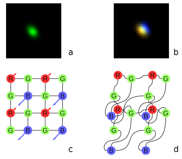
Fig. 1. Lateral chromatic aberration and Bayer mosaic: a) monochrome (green) PSF, b) composite color PSF, c) Bayer mosaic of the sensor, d) distorted mosaic for the chromatic aberration of b).
De-mosaic processing and chromatic aberrationsOur current cameras role is to preserve the raw sensor data while providing some moderate compression, all the image correction is applied during post-processing. Handling the lens aberration has to be done before color conversion (or de-mosaicing). When converting Bayer data to color images most cameras start with the calculation of the “missing” colors in the RG/GB pattern using 3×3 or 5×5 kernels, this procedure relies on the specific arrangement of the color filters.
Each of the red and blue pixels has 4 green ones at the same distance (pixel pitch) and 4 of the opposite (R for B and B for R) color at the equidistant diagonal locations. Fig.1. shows how lateral chromatic aberration disturbs these relations.
Fig.1a is the point-spread function (PSF) of the green channel of the sensor. The resolution of the PSF measurement is twice higher than the pixel pitch, so the lens is not that bad – horizontal distance between the 2 greens in Fig.1c corresponds to 4 pixels of Fig.1a. It is also clearly visible that the PSF is elongated and the radial resolution in this part of the image is better than the tangential one (lens center is left-down).
Fig.1b shows superposition of the 3 color channels: blue center is shifted up-and-right by approximately 2 PSF pixels (so one actual pixel period of the sensor) and the red one – half-pixel left-and-down from the green center. So the point light of a star, centered around some green pixel will not just spread uniformly to the two “R”s and two “B”s shown connected with lines in Fig.1c, but the other ones and in different order. Fig.1d illustrates the effective positions of the sensor pixels that match the lens aberration.
Aberrations correction at post-processing stageWhen we perform off-line image correction we start with separating each color channel and re-sampling it at twice the pixel pitch frequency (adding zero sample between each measured one) – this increase allows to shift image by a fraction of a pixel both preserving resolution and not introducing the phase errors that may be visually OK but hurt when relying on sub-pixel resolution during correlation of images.
Next is the conversion of the full image into the overlapping square tiles to the frequency domain using 2-d DFT, then multiplication by the inverted PSF kernels – individual for each color channel and each part of the whole image (calibration procedure provides a 2-d array of PSF kernels). Such multiplication in the frequency domain is equivalent to (much more computationally expensive) image convolution (or deconvolution as the desired result is to reduce the effect of the convolution of the ideal image with the PSF of the actual lens). This is possible because of the famous convolution-multiplication property of Fourier transform and its discrete versions.
After each color channel tile is corrected and the phases of color components match (lateral chromatic aberration is compensated) it is the time when the data may be subject to non-linear processing that relies on the properties of the images (like detection of lines and edges) to combine the color channels trying to achieve highest spacial resolution and not to introduce color artifacts. Our current software performs it while data is in the frequency domain, before the inverse Fourier transform and merging the lapped tiles to the restored image.
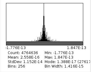
Fig.2. Histogram of difference between original image and after direct and inverse MDCT (with 8×8 pixels DCT-IV)
MDCT of an image – there and back againIt would be very appealing to use DCT-based MDCT instead of DFT for aberration correction. With just 8×8 point DCT-IV it may be possible to calculate direct 16×16 -> 8×8 MDCT and 8×8 -> 16×16 IMDCT providing perfect reconstruction of the image. 8×8 pixels DCT should be able to handle convolution kernels with 8 pixel radius – same would require 16×16 pixels DFT. I knew there will be a challenge to handle non-symmetrical kernels but first I gave a try to a 2-d MDCT to convert and reconstruct back a camera image that way. I was not able to find an efficient Java implementation of the DCT-IV so I had to write some code following the algorithms presented in [1].
That worked nicely – when I obtained a histogram of the difference between the original image (pixel values were in the range of 0 to 255) and the restored one – IMDCT(MDCT(original)) it demonstrated negligible error. Of course I had to discard 8 pixel border of the image added by replication before the procedure – these border pixels do not belong to 4 overlapping tiles as all internal ones and so can not be reconstructed.
When this will be done in the camera FPGA the error will be higher – DCT implementation there uses just an integer DSP – not capable of the double precision calculations as the Java code. But for the small 8×8 transformations it should be rather easy to manage calculation precision to the required level.
Convolution with MDCTIt was also easy to implement a low-pass symmetrical filter by multiplying 8×8 pixel MDCT output tiles by a DCT-III transform of the desired convolution kernel. To convolve f ☼ g you need to multiply DCT_IV(f) by DCT_III(g) in the transform domain [2], but that does not mean that DCT-III has also be implemented in the FPGA – the de-convolution kernels can be prepared during off-line calibration and provided to the camera in the required form.
But not much more can be done for the convolution with asymmetric kernels – they either require additional DST (so DCT and DST) of the image and/or padding data with extra zeros [3],[4] – all that reduces advantage of DCT compared to DFT. Asymmetric kernels are required for the lens aberration corrections and Fig.1 shows two cases not easily suitable for MDCT:
- lateral chromatic aberrations (or just shift in the image domain) – Fig.1b and
- “diagonal” kernels (Fig.1a) – not an even function of each of the vertical and horizontal axes.
Fig.3. Convolution kernel factorization: a) required asymmetrical and shifted kernel, b) 4-point direct convolution with (sparse) Bayer color channel data, c) symmetric convolution kernel for MDCT, d) symmetric kernel – DCT-III of c) to multiply DCT-IV kernels of the image.
Symmetric kernels are like what you can do with a twice folded piece of paper, cut to some shape and unfolded, with folds oriented strictly vertically and horizontally.
Factorization of the convolutionAnother way to handle convolution with non-symmetrical kernels is to split it in two – first convolve with an asymmetrical one directly and then – use MDCT and symmetrical kernel. The input data for combined convolution is split Bayer data, so each color channel receives sparse sequence – green one has only half non-zero elements and red and blue – only 1/4 such pixels. In the case of half-pixel grid (to handle fraction-pixel shifts) the relative amount of non-zero pixels is four times smaller, so the total number of multiplications is the same as for the whole-pixel grid.
The goal of such factorization is to minimize the number of the non-zero elements in the asymmetrical kernel, imposing no restrictions on the symmetrical one. Factorization does not have to be absolutely precise – the effect of deconvolution is limited by several factors, most important being the amplification of the sensor noise (such as shot noise). The required number of non-zero pixel may vary with the type of the distortion, for the lens we experimented with (Sunex DSL227 fisheye) just 4 pixels were sufficient to achieve 2-4% error for each of the kernel tiles. Four pixel kernels make it 1 multiplication per each of the red and blue pixels and 2 multiplications per green. As the kernels are calculated during the camera off-line calibration it should be possible to simultaneously generate scheduling of the the DSP and buffer memories to additionally reduce the required run-time FPGA resources.
Fig.3 illustrates how the deconvolution kernel for the aberration correction is split into two for the consecutive convolutions. Fig.1a shows the required deconvolution kernel determined during the existing calibration procedure. This kernel is shown far off-center even for the green channel – it appeared near the edge of the fish-eye lens field of view as the current lens model is based on the radial polynomial and is not efficient for the fish-eye (f-theta) lenses, so aberration correction by deconvolution had to absorb that extra shift. As the convolution kernel has fixed non-zero elements, the computation complexity does not depend on the maximal kernel dimensions. Fig.3b shows the determined asymmetric convolution kernel of 4 pixels, and Fig.3c – the kernel for symmetric convolution with MDCT, the unique 8×8 pixels part of it (inside of the red square) is replicated to the other3 quadrants by mirroring along row 0 and column 0 because of the whole pixel even symmetry – right boundary condition for DCT-III. Fig.3d contains result of the DCT-III applied to the data shown in Fig.3c.
Fig.4. Symmetric convolution kernel tiles in MDCT domain. Full image (click to open) has peripheral kernels replicated as there was no calibration data outside of the fisheye lens filed of view
There should be some more efficient ways to find optimal combinations of the two kernels, currently I used a combination of the Levenberg-Marquardt Algorithm (LMA) that minimizes approximation error (root mean square of the differences between the given kernel and the result of the convolution of the two calculated) and adding/replacing pixels in the asymmetrical kernel, sorting the variants for the best LMA fit. Experimental code (FactorConvKernel.java) for the kernel calculation is in the same GitHub repository.
Each kernel tile is processed independently of the neighbors, so while the aberration deconvolution kernels are changing smoothly between the adjacent tiles, the individual asymmetrical (for direct convolution with Bayer signal data) and symmetrical (for convolution by multiplication in the MDCT space) may change dramatically (see Fig.4). But when the direct convolution is applied before the window multiplication to the source pixels that contribute to a 16×16 pixel MDCT overlapping tile, then the result (after IMDCT) depends on the convolution of the two kernels, not the individual ones.
Deconvolving the test imageNext step was to apply the convolution to the test image, see if there are any visible blocking (or other) artifacts and if the image sharpness was improved. Only a single (green) channel was tested as there is no DCT-based color conversion code in this program yet. Program was tested with the whole pixel grid (not half pixel) so some reduction of sharpness caused by fractional pixel shift was expected. For the comparison “before/after” aberration correction I used two pairs – one with the raw Bayer data (half of the pixels are black in a checker-board pattern) and the other – with the Bayer pattern after 0.4 pix low-pass filter to reduce the checkerboard pattern. Without this filtering image would be either twice darker or (as on these pictures) saturated at lower levels (checkerboard 0/255 alternating pixels result in average gray level of only half of the full range).
Fig.5. Alternating images of a segment (green channel only): low-pass filter of the Bayer mosaic before and after deconvolution. Click image to show comparison with raw Bayer component.
Raw Bayer
Bayer data, low pass filter, sigma = 0.4 pix
Deconvolved
Fig.5 shows animated GIF of a fraction of the whole image, clicking the image shows comparison to the raw Bayer (with the limited gray level), caption links the full size images for these 3 modes.
No de-noise code is used, so amplification of the pixel shot noise is clearly visible, especially on the uniform surfaces, but aliasing cancellation remained functional even with abrupt changing of the convolution kernels as ones shown in Fig.4.
ConclusionsAlgorithms suitable for FPGA implementation are tested with the simulation code. Processing of the images subject to the typical optical aberration of the fisheye lens DSL227 does not add significantly to the computational complexity compared to the pure symmetric convolution using lapped MDCT based on the 8×8 pixels two-dimensional DCT-IV.
This solution can be used as a first stage of the real time image correction and rectification, capable of sub-pixel resolution in multiple application areas, such as 3-d reconstruction and autonomous navigation.
References [1] Plonka, Gerlind, and Manfred Tasche. “Fast and numerically stable algorithms for discrete cosine transforms.” Linear algebra and its applications 394 (2005): 309-345.
[2] Martucci, Stephen A. “Symmetric convolution and the discrete sine and cosine transforms.” IEEE Transactions on Signal Processing 42.5 (1994): 1038-1051. pdf
[3] Suresh, K., and T. V. Sreenivas. “Linear filtering in DCT IV/DST IV and MDCT/MDST domain.” Signal Processing 89.6 (2009): 1081-1089. Abstract and full text pdf.
[4] Reju, Vaninirappuputhenpurayil Gopalan, Soo Ngee Koh, and Ing Yann Soon. “Convolution using discrete sine and cosine transforms.” IEEE Signal Processing Letters 14.7 (2007): 445. pdf
[5] Malvar, Henrique S. “Extended lapped transforms: Properties, applications, and fast algorithms.” IEEE Transactions on Signal Processing 40.11 (1992): 2703-2714.
Measuring SSD interrupt delays
Sometimes we need to test disks connected to camera and we developed a small test program for this purpose. This program basically resembles camogm (in-camera recording program) in its operation and allows us to write repeating blocks of data containing counter value and then check the consistency of the data written. This program works directly with disk driver and collects some statistics during its operation. Disk driver, among other things, measures the time between two events: when write command is issued and when command completion interrupt from controller is received. This time can be used to measure disk write speed as the amount of data sent to disk with each command is also known. In general, this time slightly floats around its average value given that the amount of data written with each command is almost the same. But long run tests have shown that sometimes the interrupt return time after write command can be much longer then the average time.
We decided to investigate this situation in a little bit more details and tested two SSDs with our test program. The disks used for tests were SanDisk SD8SMAT128G1122 and Crucial CT250MX200SSD6, both were connected to eSATA camera port over M.2 SSD adapter. We used these disks before and they demonstrated different performance during recording. We ran camogm_test to write 3 MB blocks of data in cyclic mode. The program collected delayed interrupt times reported by driver as well as the amount of data written since the last delay event. The processed results of the test are in the following table:
Disk Average IRQ reception time, ms Standard deviation, ms Average IRQ delay time, ms Standard deviation, ms Data recorded since last IRQ delay, GB Standard deviation, GB CT250MX200SSD6 (250 GB) 11.9 1.1 804 12.7 499.7 111.7 SD8SMAT128G1122 (128 GB) 19.3 4.8 113 6.5 231.5 11.5The delayed interrupt times of these disks are considerably different although the difference in average interrupt times which reflect disk write speeds is not that big. It is interesting to notice that the amount of data written to disk between two consecutive interrupt delays is almost twice the total disk size. smartctl reported the increase of Runtime_Bad_Block attribute for CT250MX200SSD6 after each delay but the delays occurred each time on different LBAs. Unfortunately, SD8SMAT128G1122 does not have such parameter in its smartctl attributes and it is difficult to compare the two disks by this parameter.
DCT type IV implementation
As we finished with the basic camera functionality and tested the first Eyesis4π built with the new 10393 system boards (it is smaller, requires less power and, is faster) we are moving forward with the in-camera image processing. We plan to combine our current camera calibration methods that require off-line post processing and the real-time image correction using the camera own FPGA resources. This project development will require switching between the actual FPGA coding and the software implementation of the same algorithms before going to the next step – software is still easier to design. The first part was in FPGA realm – it was to implement the fundamental image processing block that we already know we’ll be using and see how much of the resources it needs.
DCT type IV as a building block for in-camera image processingWe consider a small (8×8 pixel) DCT-IV to be a universal block for conditioning of the raw acquired images. Such operations as lens optical aberrations correction, color conversion (de-mosaic) in the presence of the lateral chromatic aberration, image rectification (de-warping) are easier to perform in the frequency domain using convolution-multiplication property and other algorithms.
In post-processing we use DFT (Discrete Fourier Transform) over rather large (64×64 to 512×512) tiles, but that would be too much for the in-camera processing. First is the tile size – for good lenses we do not need that large convolution kernels. Additionally we plan to combine several processing steps into one (based on our off-line post-processing experience) and so we do not need to sub-sample images – in our current software we double resolution of the raw images at the beginning and scale back the final result to reduce image degradation caused by re-sampling.
The second area where we plan to reduce computations is the replacement of the DFT with the DCT that is designed to be fed with the pure real data and so requires less arithmetic operations than DFT that processes complex input values.
Why “type IV” of the DCT?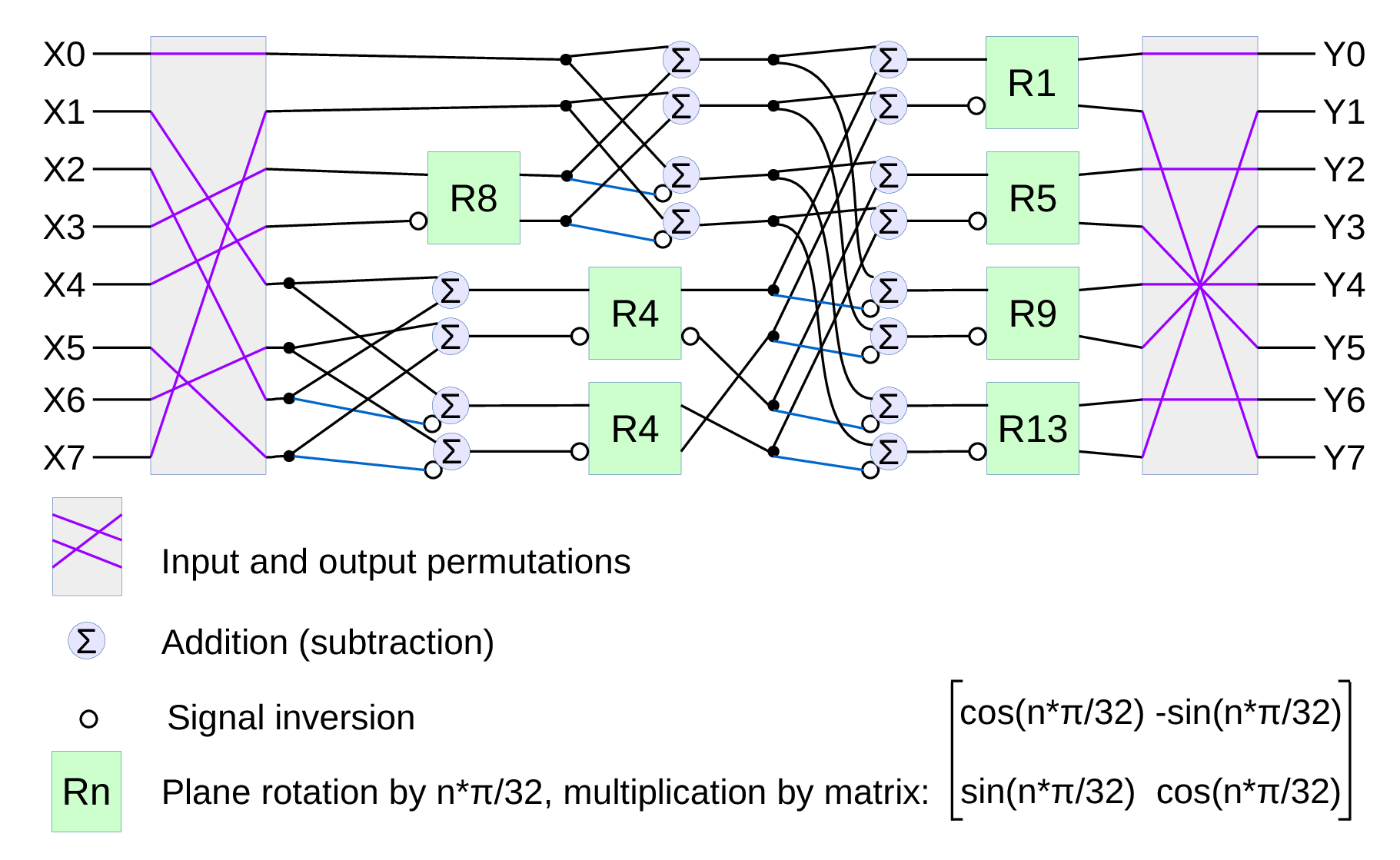
Fig.1. Signal flow graph for DCT-IV
We already have DCT type II implemented for the JPEG/JP4 compression, and we still needed another one. Type IV is used in audio compression because it can be converted to a modified discrete cosine transform (MDCT) – a procedure when multiple overlapped windows are processed one at a time and the results are seamlessly combined without any block artifacts that are familiar for the JPEG with low settings of the compression quality. We too need lapped transform to process large images with relatively small (much smaller than the image itself) convolution kernels, and DCT-IV is a perfect fit. 8-point DCT-IV allows to implement transformation of 16-point segments with 8-point overlap in a reversible manner – the inverse transformation of 8-point data may be converted to 16-point overlapping segments, and being added together these segments result in the original data.
There is a price though to pay for switching from DFT to DCT – the convolution-multiplication property being so straightforward in FFT gets complicated for DCT[1]. While convolving with symmetrical kernels is still simple (just the kernel has to be transformed differently, but it is anyway done off-line in our case), the arbitrary kernel convolution (or just a shift in image space needed to compensate the lateral chromatic aberration) requires both DCT-IV and DST-IV transformed data. DST-IV can be calculated with the same DCT-IV modules (just by reversing the direction of input data and alternating the sign of the output samples), but it still requires additional hardware resources and/or more processing time. Luckily it is only needed for the direct (image domain to frequency domain) transform, the inverse transform IDCT-IV (frequency to image) does not require DST. And IDCT-IV is actually the same as the direct DCT-IV, so we can again instantiate the same module.
Most of the two-dimensional transforms combine 1-d transform modules (because DCT is a separable transform), so we too started with just an 8-point DCT. There are multiple known factorizations for such algorithm[2] and we used one of them (based on BinDCT-IV) shown in Fig.1.
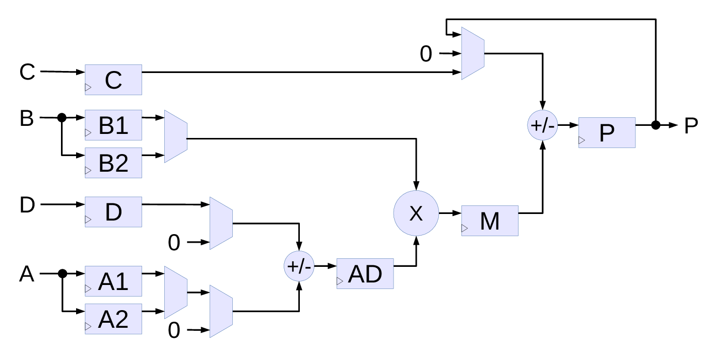
Fig.2. Simplified diagram of Xilinx DSP48E1 primitive (only used functionality is shown)
DSP primitive in Xilinx ZynqThis algorithm is implemented with a pair of DSP48E1[3] primitives shown in Fig.2. This primitive is flexible and allows to configure different functionality, the diagram contains only the blocks and connections used in the current project. The central part is the multiplier (signed 18 bits by signed 25 bits) with inputs from a pair of multiplexed B registers (B1 and B2, 18 bits wide) and the pre-adder AD register (25 bits). The AD register stores sum/difference of the 25-bit D-register and a multiplexed pair of 25-bit A1 and A2 registers. Any of the inputs can be replaced by zero, so AD can receive D, A1, A2, -A1, -A2, D+A1, D-A1, D+A2 and D-A2 values. Result of the multiplier (43 bits) is stored in the M register and the data from M is combined with the 48-bit output accumulator register P. Final adder can add or subtract M to/from one of the P, 48-bit C-register or just 0, so the output P register can receive +/-M, P+/-M and C+/-M. The wrapper module dsp_ma_preadd_c.v reduces the number of DSP48E1 signals and parameters to those required for the project and in addition to the primitive instance have a simple model of the DSP slice to allow simulation without the DSP48E1 source code for convenience.
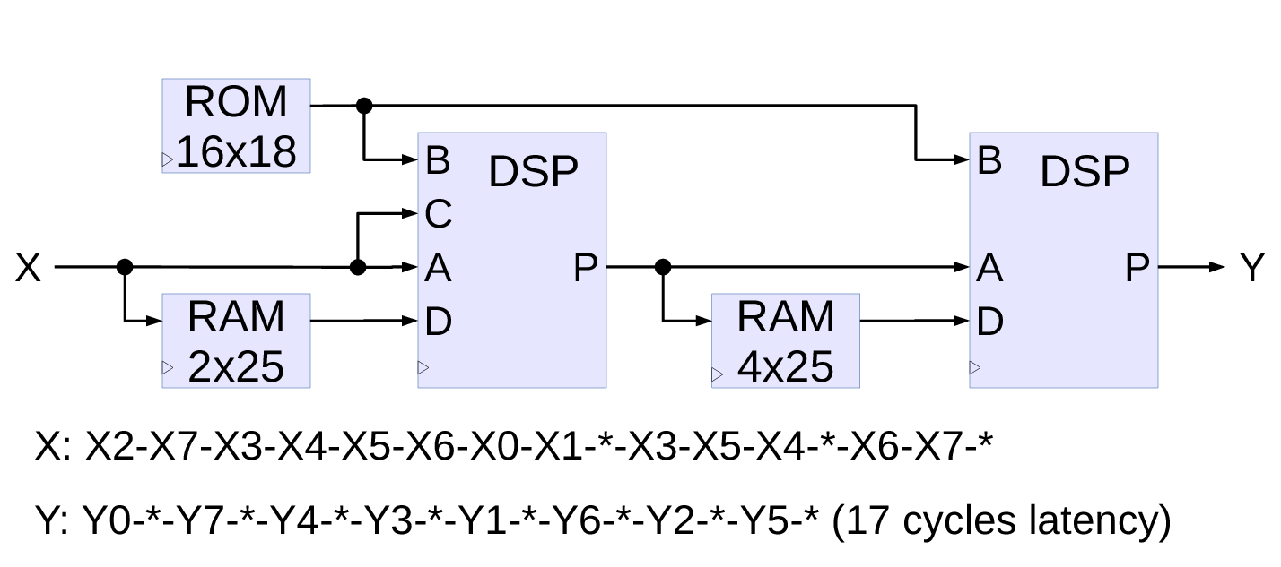
Fig.3. One-dimensional 8-point DCT-IV implementation
8-point DCT-IV transformThe DCT-IV implementation module (Fig.3.) operates in 16 clocks cycles (2 clock periods per data item) and the input/output permutations are not included – they can be absorbed in the data source and destination memories. Current implementation does not implement correct rounding and saturation to save resources – such processing can be added to the outputs after analysis for particular application data widths. This module is not in the coder/decoder signal chain so bit-accuracy is not required.
Data is output each other cycle (so two such modules can easily be used to increase bandwidth), while input data is scrambled more, some of the items have to appear twice in a 16-cycle period. This implementation uses two of the DSP48E1 primitives connected in series. First one implements the left half of the Fig.1. graph – 3 rotators (marked R8, and two of R4), four adders, and four subtracters, The second one corresponds to the right half with R1, R5, R9, R13, four adders, and four subtracters. Two of the small memories (register files) – 2 locations before the first DSP and 4 locations before the second effectively increase the number of the DSP internal D registers. The B inputs of the DSPs receive cosine coefficients, the same ROM provides values for both DSP stages.
The diagram shows just the data paths, all the DSP control signals as well as the memories write and read addresses are generated at the defined times decoded from the 16-cycle period. The decoder is based on the spreadsheet draft of the design.
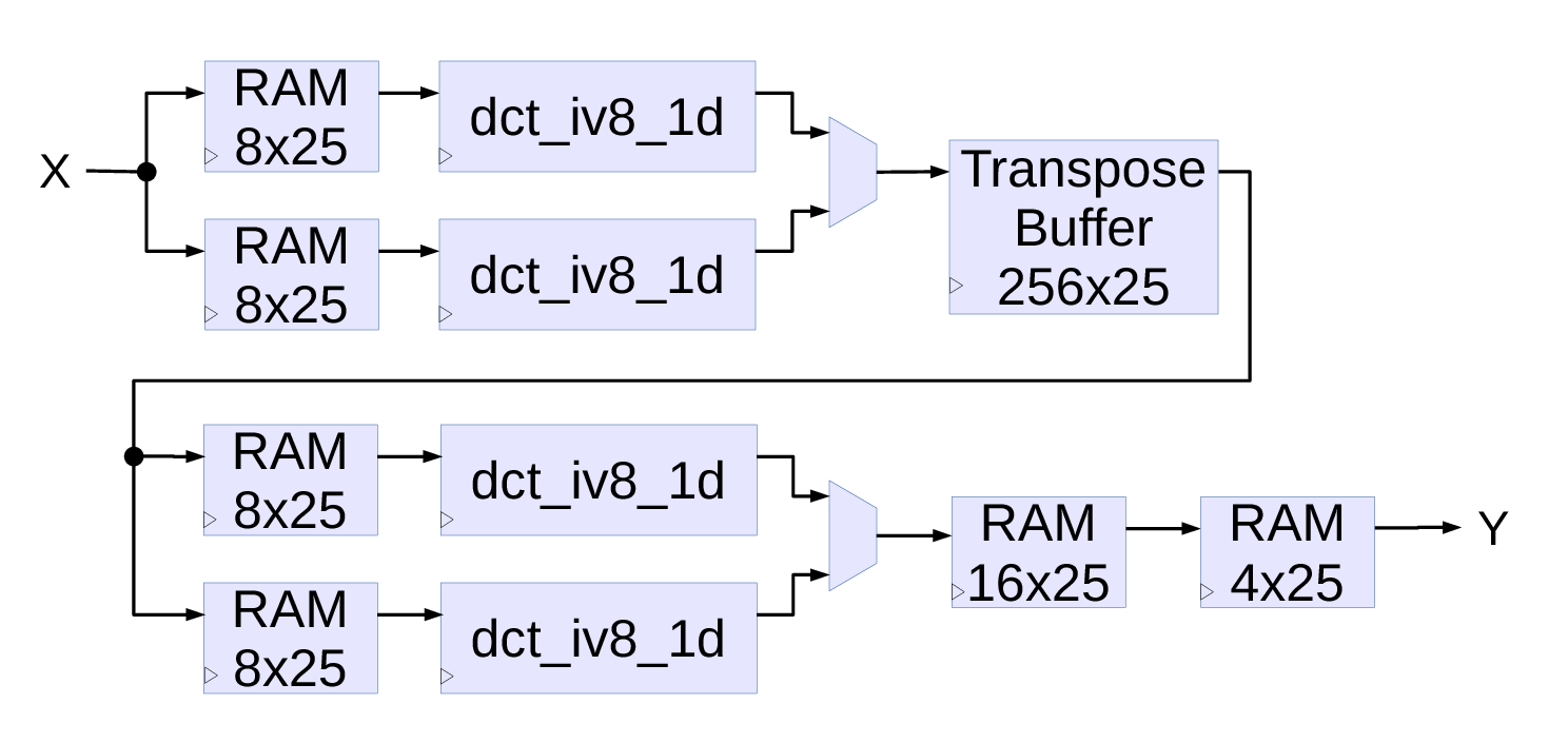
Fig.4. Two-dimensional 8×8 DCT-IV
Two-dimensional 8×8 points DCT-IVNext diagram Fig.4. show a two-dimensional DCT type IV implementation using four of the 1-d 8-point DCT-IV modules described above. Input data arrives continuously in line-scan order, next 64-item block may follow either immediately or after a delay of at least 16 cycles so the pipelines phases are correctly restarted. Two of the input 8×25 memories (width can be reduced to match input data, 25 is the width of the DSP48E1 inputs) are used to re-order the input data.As each of the 1-d DCT modules require input data at more than a half cycles (see bottom of Fig.3) interleaving with the common memory for both channels is not possible, so each channel has to have a dedicated one. First of the two DCT modules convert even lines of 8 points, the other one – odd lines. The latency of the data output from the RAM in the second channel is made 1 cycle longer, so the output data from the channels also arrive at odd/even time slots and can be multiplexed to a common transpose buffer memory. Minimal size of the buffer is 2 of the 64 item pages (width can be reduced to match application requirements), but having just a two-page buffer increases the minimal pause time between blocks (if they are not immediate), with a four page buffer (and BRAM primitives are larger even if just halves are used) the minimal non-immediate delay of the 16 cycles of a 1-d module is still valid.
The second (vertical) pass is similar to the first (horizontal) one, it also has individual small memories for input data reordering and 2 output de-scrambler memories. It is possible to use a single stage, but the memory should hold at least 17 items (>16) and the primitives are 16-deep, and I believe that splitting in series makes it easier for the placer/router tools to implement the design.
Next stepsNow when the 8×8 point DCT-IV is designed and simulated the next step is to switch to the Java coding (add to our ImageJ plugin for camera calibration and image post-processing), convert calibration data to the form suitable for the future migration to FPGA and try the processing based on the chosen 8×8 DCT-IV. When satisfied with the results – continue with the FPGA coding.
References[1] Martucci, Stephen A. “Symmetric convolution and the discrete sine and cosine transforms.” IEEE Transactions on Signal Processing 42.5 (1994): 1038-1051. pdf
[2] Rao, K. Ramamohan, and Ping Yip. Discrete cosine transform: algorithms, advantages, applications. Academic press, 2014.
[3] 7 Series DSP48E1 Slice, UG479 (v1.9), Xilinx, Sep. 2016. pdf
Using a flash with a CMOS image sensor: ERS and GRR modes
Operation modes in conventional CMOS image sensors with the electronic rolling shutter
Further, I will be writing about ON Semi’s MT9P001 image sensor focusing on snapshot modes. The operation modes are described in the sensor’s datasheet. In short:
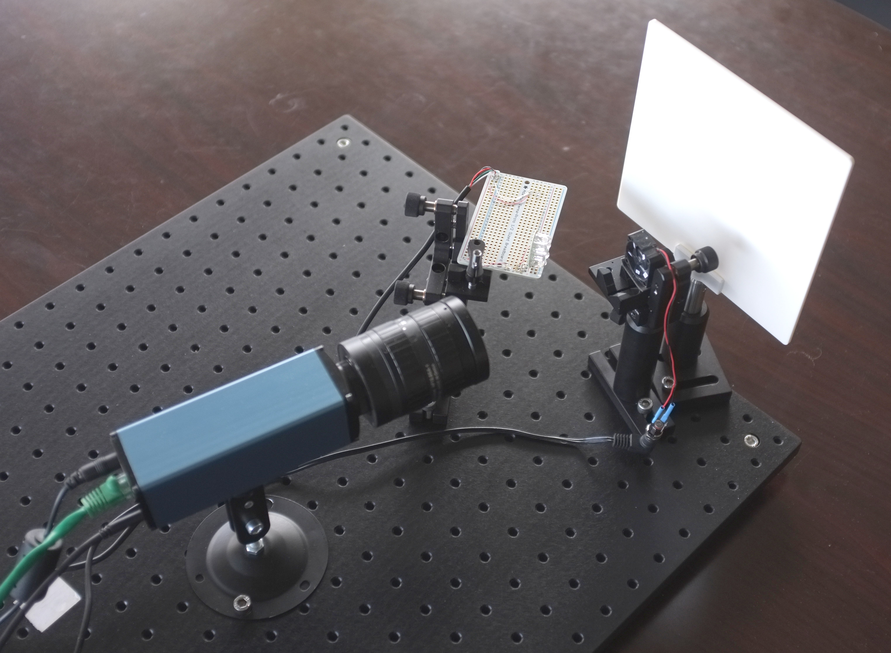
Flash test setup
Most of the CMOS image sensors have Electronic Rolling Shutter – the images are acquired by scanning line by line. Their strengths and weaknesses are well known and extremely wide usage made the technology somewhat perfect – Andrey might have already said this somewhere before.
There are CMOS sensors with a Global Shutter but (for the same formats) their pixels’ dynamic range is lower, the readout noise is bigger and the frame rates are lower as well. Here are a few links:
- CCD and CMOS Sensor Architecture and Readout Modes (nice pictures)
- Rolling vs Global Shutter
- Rolling Shutter (Wikipedia)
So, the typical sensor with ERS may support 3 modes of operation:
- Electronic Rolling Shutter (ERS) Continuous
- Electronic Rolling Shutter (ERS) Snapshot
- Global Reset Release (GRR) Snapshot
GRR Snapshot was available in the 10353 cameras but ourselves we never tried it – one should have write directly to the sensor’s register to turn it on. But now it is tested and working in 10393s available through the TRIG (0x14) parameter.
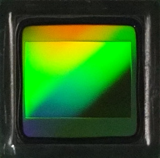
MT9P001 sensor
Further, I will be writing about ON Semi’s MT9P001 image sensor focusing on snapshot modes. The operation modes are described in the sensor’s datasheet. In short:
In ERS Snapshot mode (Fig.1,3), exposure time is constant across all rows but each next row’s exposure start is delayed by tROW (row readout time) from the previous one (and so is the exposure end).
In GRR Snapshot mode (Fig.2,4), the exposure of all rows starts at the same moment but each next row is exposed by tROW longer than the previous one. This mode is good when a flash use is needed.
The difference between ERS Snapshot and Continuous is that in the latter mode the sensor doesn’t wait for a trigger and starts new image while still finishing reading the previous one. It provides the highest frame rate (Fig.5).
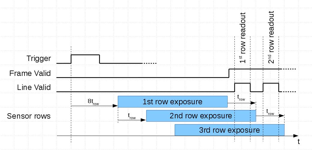
Fig.1 Electronic Rolling Shutter (ERS) Snapshot mode
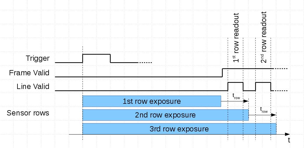
Fig.2 Global Reset Release (GRR) Snapshot mode
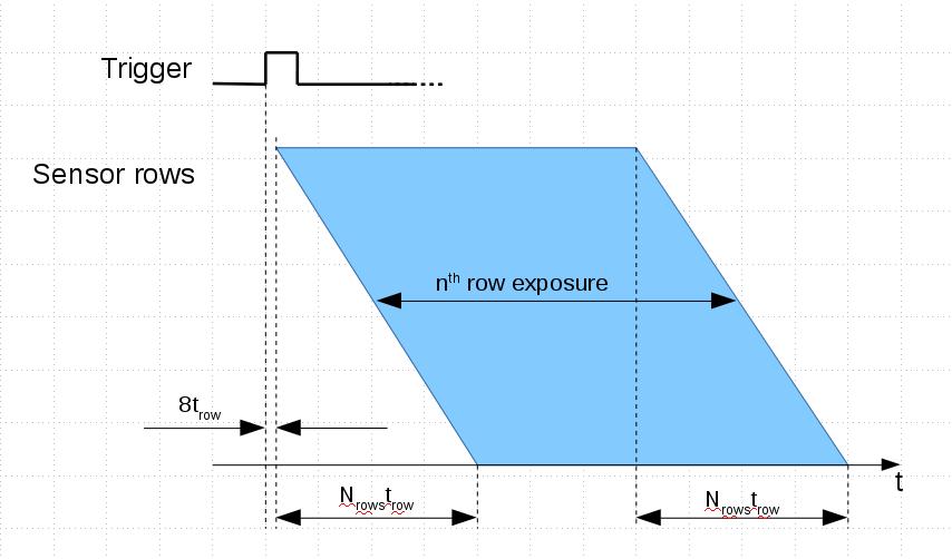
Fig.3 ERS mode, whole frame
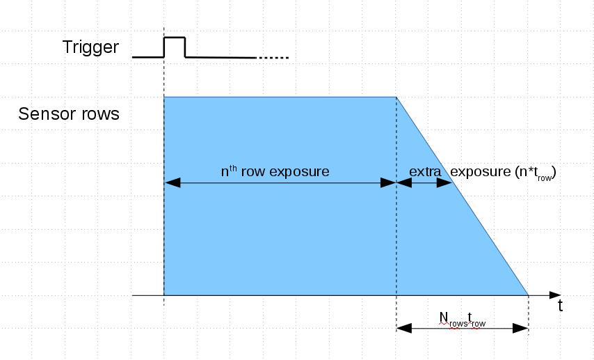
Fig.4 GRR mode, whole frame
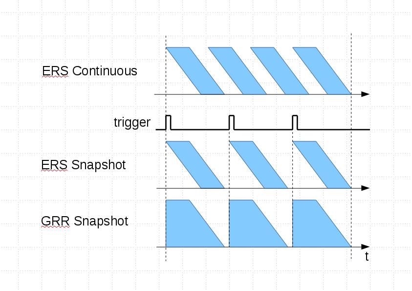
Fig.5 Sensor operation modes, frame sequence
Here are some of the actual parameters of MT9P001:
Parameter Value Active pixels 2592h x 1944v tROW 33.5 μs Frame readout time (Nrows x tROW) 1944 x 36.38 μs ~ 72 ms Test setup- NC393L-389
- 9xLEDs
- Fan (Copal F251R, 25×25 mm, rotating at 5500-8000 RPM)
The LEDs were powered & controlled by the camera’s external trigger output, the delay and duration of which are programmable.
The flash duration was set to 20 μs to catch, without the motion blur, the fan’s blades are marked with stickers – 5500-8000 RPM that is 0.5-0.96° per 20 μs. There was not enough light from the LEDs, so the setup is placed in dark environment and the camera color gains were set to 8 (ISO ~800-1000) – the images are a bit noisy.
The trigger period was set to 250 ms – and the synced LEDs were blinking for each frame.
The information on how to program the NC393 camera to generate trigger signal, fps, change sensor’s operation modes (ERS/GRR) can be found here.
Fig.6a Setup: screen, camera view
Fig.6b Setup: fan
Fig.6c Setup: fan, camera view
Flash in ERS mode Fig.7a Fig.7b Fig.7c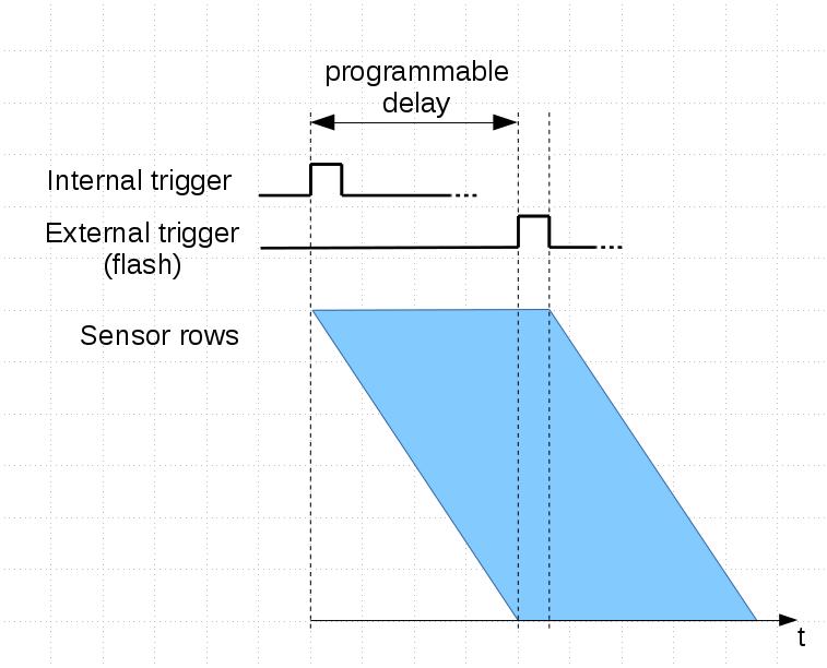
In Fig.7a to expose all rows to the flash the exposure needs to be programmed so the 1st row’s end of exposure will exceed the last row’s start of exposure and the flash delayed until the exposure start of the last row. That makes the single row exposure 72ms+tflash.
Note: there is no ERS effect for moving objects – provided, of course, that the flash is much brighter than the other light sources that will be reducing the contrast during the 72ms frame time.
In Fig.7b the exposure is shorter than the frame readout time – the flash delay can be any – the result is a brighter band on the image as shown in the example below.
Another way to expose all rows is to keep the flash on from the 1st row start until the last row end (Fig.7c) – that’s as good as keeping the flash on all the time.
Example:
Diagram Screen Fan Exposure time, ms 5 20 Flash duration, ms 0.02 (20μs) 0.02 Flash delay, ms 40 40 Comments The fan blades are motion blurred in the rows not affected by the delayed 20μs flash. The flash delay is set so the affected rows appear in the middle of the image. Exposure time defines the width of the bright rows band. Flash in GRR mode Fig.8a Fig.8b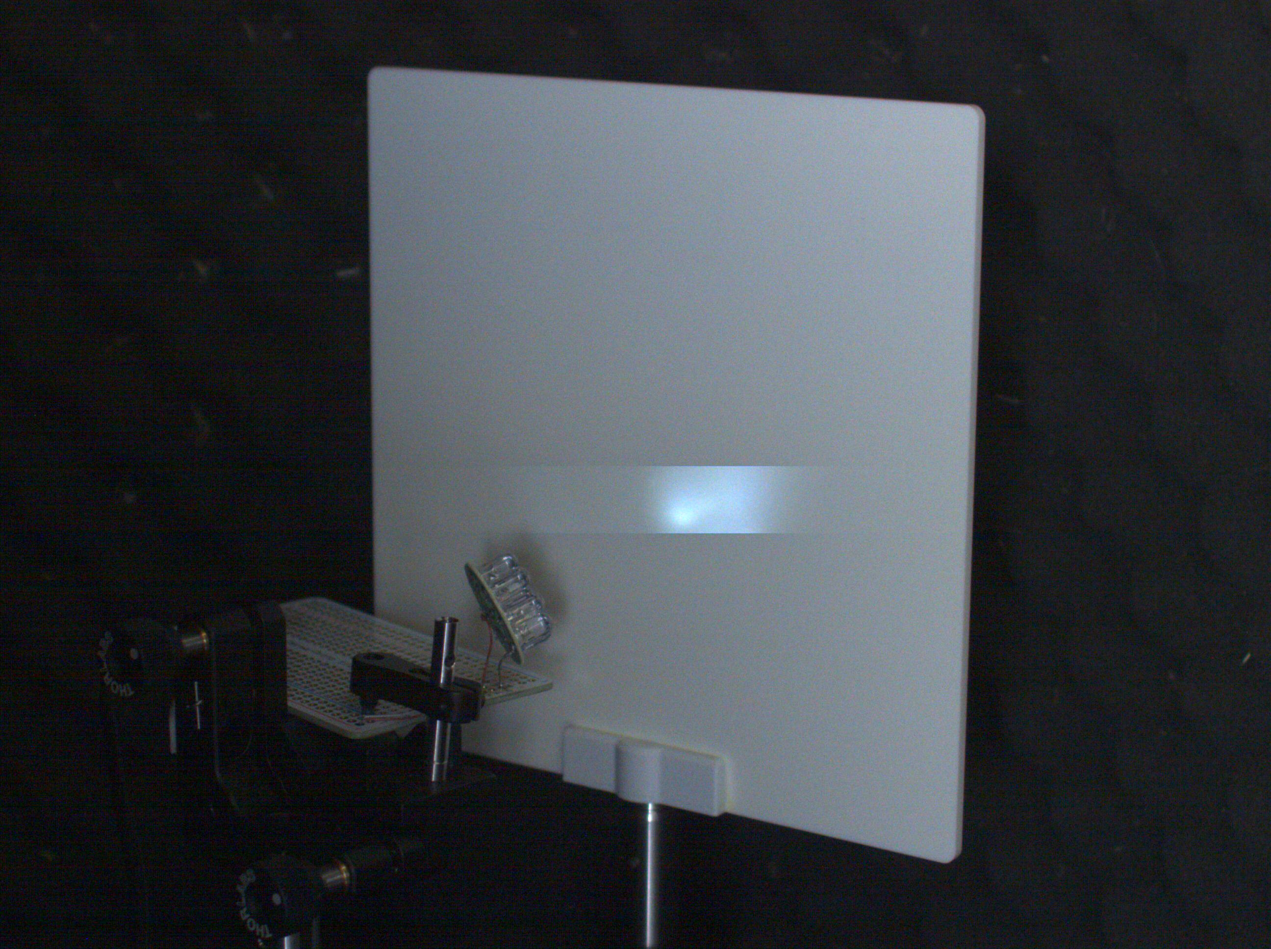
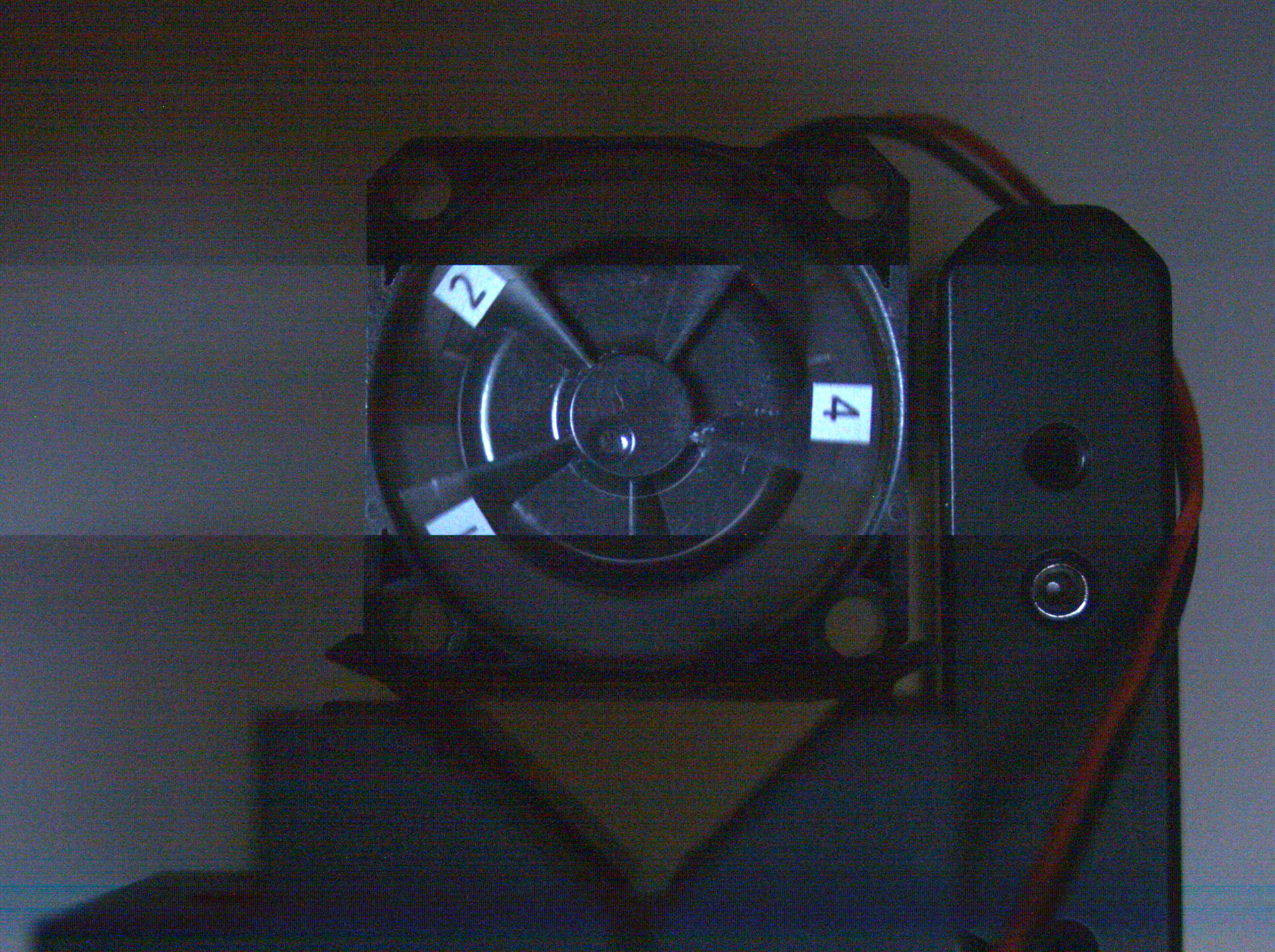
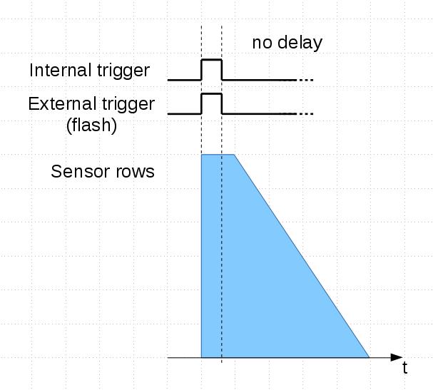
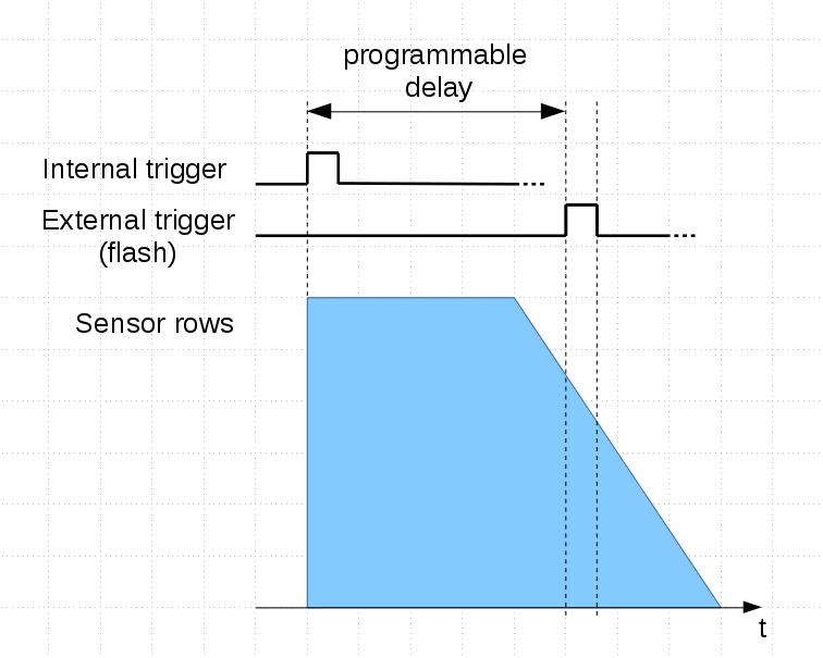
In GRR mode the flash does not need to be delayed and the exposure of the 1st row can be as low as tflash but the last row will be exposed for tflash+72ms (Fig.8a). If the scene is uniformly illuminated the the image tends to be darker in the top and getting brighter in the bottom. GRR is very useful with a flash lamp.
Note: No ERS effect (as in Fig.7a case).
Fig.8b just shows what happens if the flash is delayed until frame is read out.
Examples:
Diagram Screen Fan Exposure time, ms 0.1 0.1 Flash duration, ms 0.02 0.02 Flash delay, ms 40 30 Comments The fan blades are motion blurred in the rows not affected by the delayed 20μs flash. All of the rows not read out before the flash are affected. Diagram Screen Fan Exposure time, ms 0.1 0.1 Flash duration, ms 0.02 0.02 Flash delay, ms 0 0 Comments Fan is rotating. No motion blur. In GRR if flash is not delayed the whole image is affected by the flash. Brighter environment = lower contrast. Diagram Screen Fan Exposure time, ms 5 10 Flash duration, ms 0.02 0.02 Flash delay, ms 0 0 Comments Fan is rotating. 100 times longer exposure compared to the previous example – the environment is relatively dark. Conclusions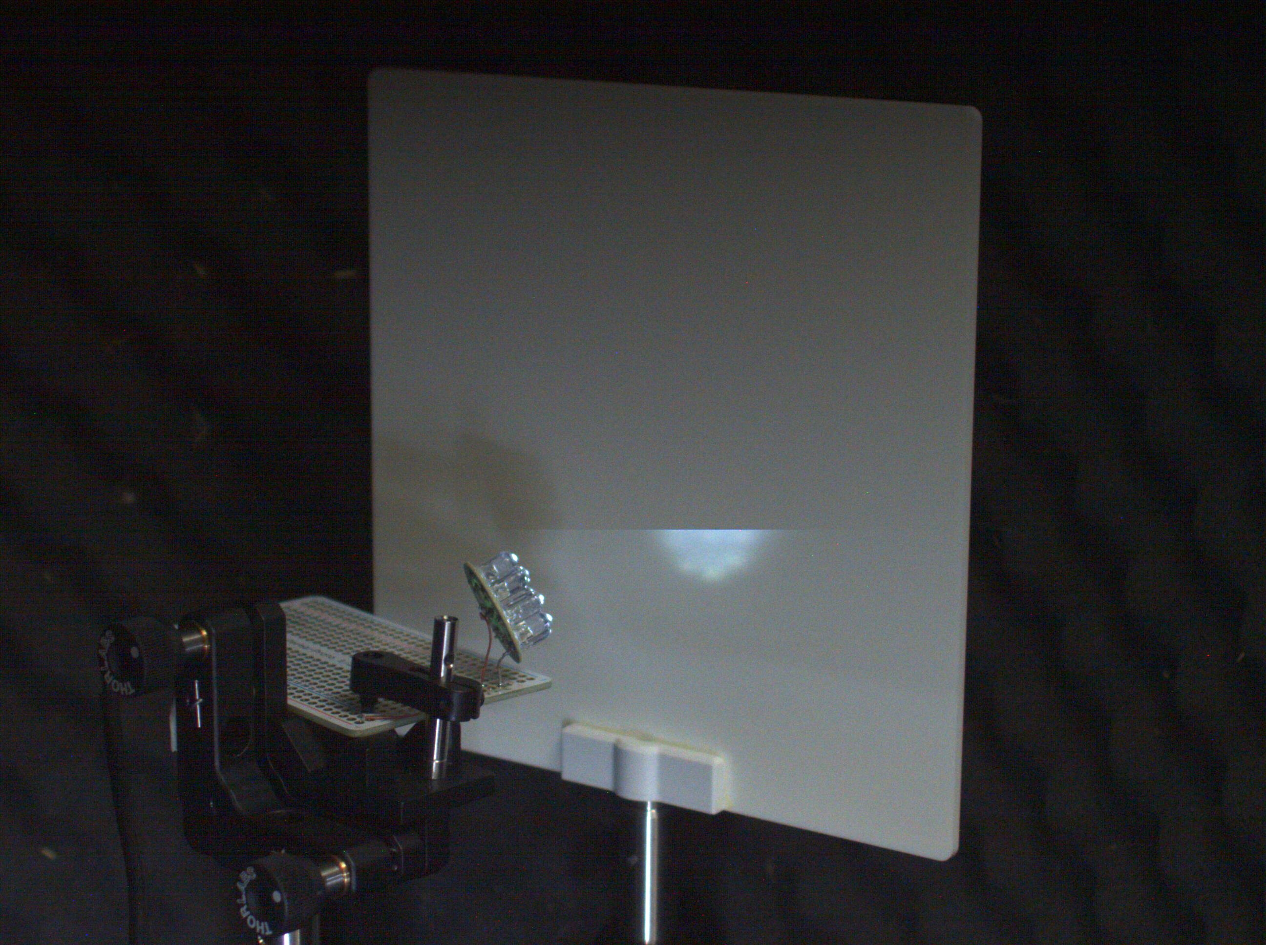
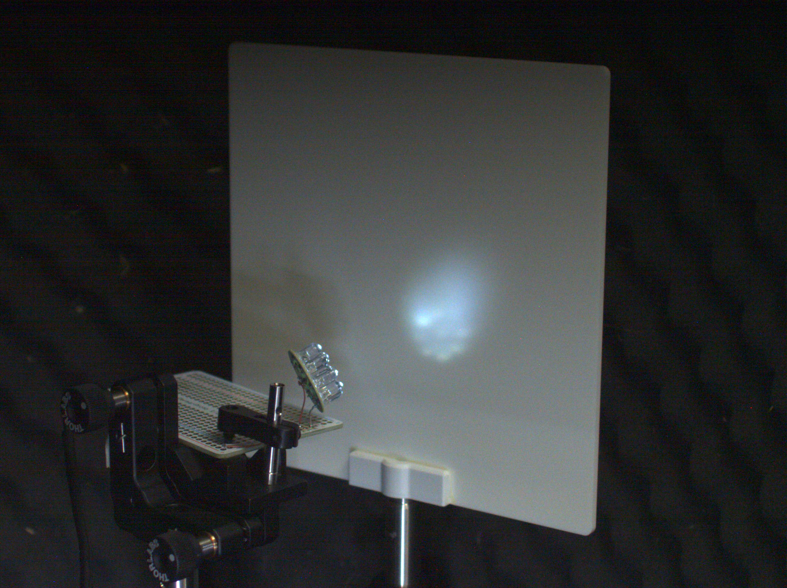
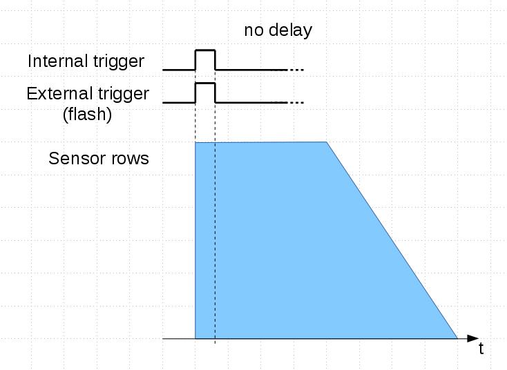
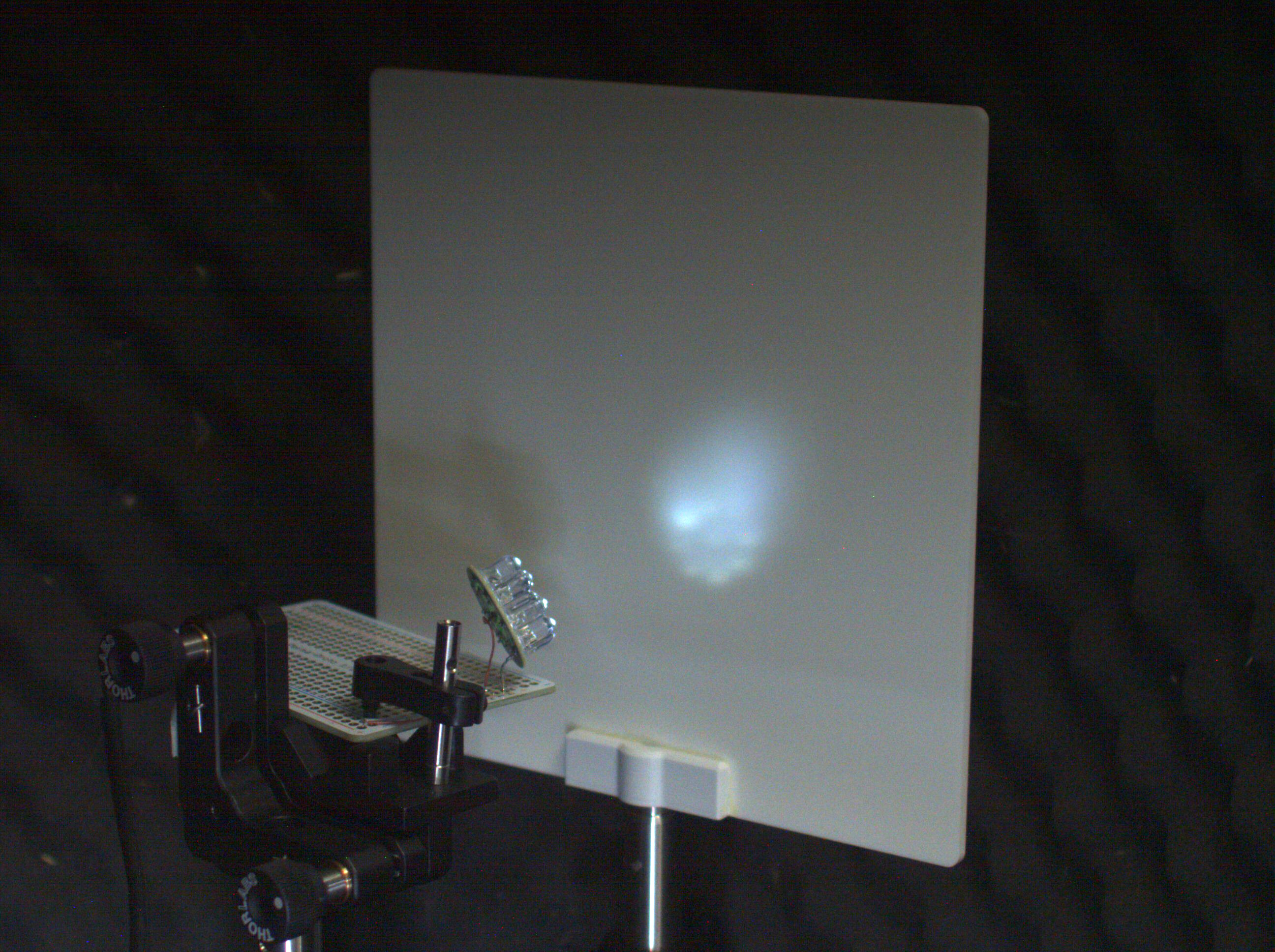
- ERS Continuous – max fps, constant exposure, not synced
- ERS Snapshot – constant exposure, synced
- GRR Snapshot – synced, use this mode with flash
- How to program 10393 parameters: ERS/GRR, fps, output trigger delay to sync with flash or else, trigger duration
Elphel presenting at ORCONF 2016, An open source digital design conference
On October 8th, 2016 Andrey will be presenting his work on VDT – Free Software Environment for FPGA Development at an open source digital design conference, ORCONF 2016. ORCONF 2016
The conference will take place in Bologna, Italy, and we are glad for the possibility to meet some of European users of Elphel cameras, and to connect with the community of developers excited about open source design, free software and open hardware.
Elphel will be present at the conference by Andrey Filippov from USA headquarters and Alexadre Poltorak, founder of Swiss 3D4Pi mobile mapping company, working closely with Elphel to integrate Eyesis4Pi, stereophotogrammetric camera, for the purpose of image based 3D reconstruction applications. Andrey will bring and demonstrate the new multisensor NC393 H-camera and Alexandre plans to take some panoramic footage with Eyesis4Pi camera, while in Bologna.
NC393 development progress and the future plans
Since we started to deliver first NC393 series cameras in May we were working on the cameras software – original version was rather limited. While it was capable of serving images/video over the network and recording them on the internal m.2 SSD, it did not have the advanced image acquisition control (through the GUI and programmatically) that was standard for the earlier NC353 series. Now the core functionality is operational and in a month we plan to have the remaining parts (inter-camera synchronization, working with multiple sensors per-port with 10359 multiplexer, GPS+IMU logging) online too. FPGA code is already ported, but it needs to be tested and a fair amount of troubleshooting, identifying the problems and weeding out the bugs is still left to be done.
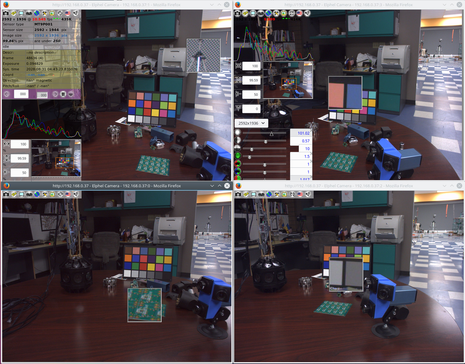
Fig 1. Four camvc instances for the four channels of NC393 camera
Users of earlier Elphel cameras can easily recognize familiar camvc web interface – Fig. 1 shows a screenshot of the four instances of this interface controlling 4 sensors of NC393 camera in “H” configuration.
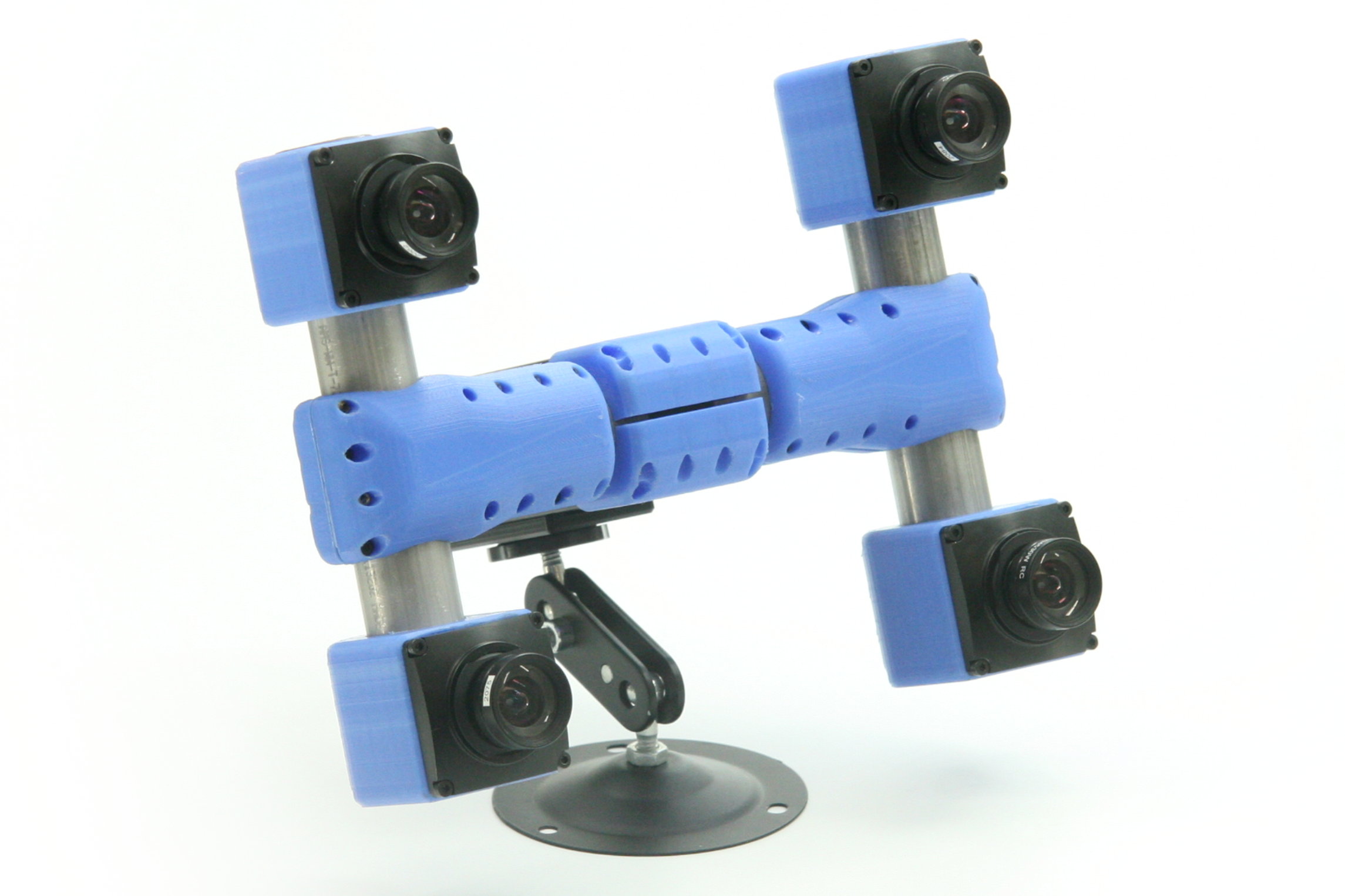
This web application tests multiple underlaying pieces of software in the camera: FPGA code, Linux kernel drivers that control the low level of the camera operation and are handling 8 interrupts from the imaging subsystem (NC353 camera processor had just one), PHP extension to interact with the drivers, image server, histograms visualization program, autoexposure and white balance daemons as well as multiple PHP scripts and Javascript code. Luckily, the higher the level, the less changes we needed in the code from the NC353 (in most cases just a single new parameter – sensor port had to be introduced), but the debugging process included going through all the levels of code – bug chasing could start from Javascript code, go to PHP code, then to PHP extension, to kernel driver, direct FPGA control from the Python code (bypassing drivers), simulating Verilog code with Cocotb. Then, when the problem was identified and the HDL code corrected (it usually required several more iterations with simulation), the top level programs were tested again with the new FPGA bitstream. And this is the time when the integration of all the development in the same Eclipse IDE is really paying off – easy code navigation, making changes to different language programs – and the software was rebuilding and transferring the results to the target system automatically.
Camera core softwareNC393 camera software aims the same goals as the previous models – allow the full speed operation of the imagers while minimizing real-time requirements to the software on the two levels:
- kernel level (tolerate large delays when waiting for the interrupts to be served) and
- application level – allow even scripting languages to keep up with the hardware
Interrupt latency is usually not a problem what working with full frame multi-megapixel images, but the camera can operate a small window at high FPS too. Many operations with the sensor (like changing resolution or image size) require coordinated updating sensor internal registers (usually over I²C connection), changing parameters of the sensor-to-memory FPGA channel (with appropriate latency), parameters of the memory-to-compressor channel, and parameters of the compressor itself. Additionally the camera software should provide the modified image headers (reflecting the new window size) when the acquired image will be recorded or requested over the network.
Application software just needs to tell when (at what frame number) it needs the new window size and the kernel plus FPGA code will take care of the rest. Slow software should just tell in advance so the camera code and the sensor itself will have enough time to execute the request. Multiple parameters modifications designated for a specific frame will be applied almost simultaneously even if frame sync pulses where received from the sensor while application was sending the new data.
Image-derived data remains available long after the image is acquiredSimilar things happen with the data received from the sensor – image itself and histograms (they are used for the automatic exposure adjustment and white balancing). Application does not need to to read them before the next frame data arrives – compressed images are kept in a large (64MB per port) ring buffer in the system memory – it can keep record of several seconds of images. Histograms (for up to 4 different windows inside the full image for each sensor port) are preserved for 15 frames after being acquired and transferred over DMA to the system memory. Subset of essential acquisition parameters and image metadata (needed for Exif output) are preserved for 2048 and 511 frames respectively.
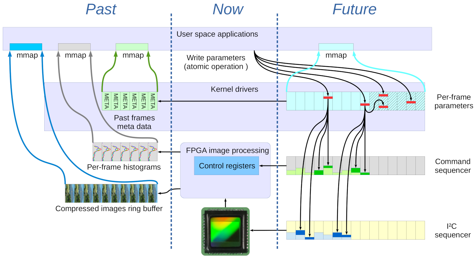
Fig 2. Interaction of the image sensor, FPGA, kernel drivers and user space applications
FPGA frame-based command sequencersThere are 2 sequencers for each of the four sensor ports on the FPGA level – they do not use any of the CPU resources:
- I²C sequencers handle relatively slow i2c commands to be sent to the senor, usually these commands need to arrive before start of the next frame,
- Command sequencers perform writes to the memory-mapped registers and so control the FPGA operation. These operations need to happen in guaranteed time just after the start of frame, before the corresponding subsystems begin to process the incoming image data.
Both are synchronized by the “start of frame” signals from the sensor, each sequencer has 16 frame pages, each page contains 64 command slots.
Sequencers allow absolute (modulo 16) frame address and relative (to current) frame address. Writing to the current frame (zero offset) is interpreted as “ASAP” and the commands are issued immediately, not synchronized by the start of frame. Additionally, if the commands were written too late and the frame sync arrived before they were executed, they will still be processed before the next frame slot page is activated.
Kernel support of the image frame parametersThere are many frame-related parameters that control image acquisition in the camera, including various sensor register settings, parameters that control gamma conversion, image format for recording to video memory (dedicated to FPGA DDR3 not shared with the CPU), compressor format, signal gains, color saturations, compression quality, coring parameters, histogram windows size and position. There is no such thing as the “current frame parameters” in the camera, at any given moment the sensor may be programmed for a certain image size, while its output data reflects the previous frame format, and the compressor is still not finished with even earlier image. That means that the camera should be aware of multiple sets of the same parameters, each applicable to a certain frame (identified by an absolute frame number). In that case the sensor “now” is receiving not the “current” frame parameters, but the frame parameters of a frame that will happen 2 frame intervals later.
Current implementation keeps parameters (all parameters are unsigned long) in a 16-element ring buffer, each element being a
/** Parameters block, maintained for each frame (0..15 in NC393) of each sensor channel */ struct framepars_t { unsigned long pars[927]; ///< parameter values (indexed by P_* constants) unsigned long functions; ///< each bit specifies function to be executed (triggered by some parameters change) unsigned long modsince[31]; ///< parameters modified after this frame - each bit corresponds to one element in in par[960] (bit 31 is not used) unsigned long modsince32; ///< parameters modified after this frame super index - non-zero elements in in mod[31] (bit 31 is not used) unsigned long mod[31]; ///< modified parameters - each bit corresponds to one element in in par[960] (bit 31 is not used) unsigned long mod32; ///< super index - non-zero elements in in mod[31] (bit 31 is not used) };Interrupt driven processing of the parameters take CPU time (in contrast with the FPGA sequencers described before), so the processing should be efficient and not iterate through almost a thousand entries for each interrupt, It is also not practical to copy a full set of parameters from the previous frame. Parameters structure for each frame include mod[31] array where each element stores a bit field that describes modification of the 32 consecutive parameters, and a single mod32 represents each mod as a single bit. So mod32 == 0 means that there were no changes (as is true for the majority of frames) and there is nothing to do for the interrupt service routine. Additional fields modsince[31] and modsince32 mean that there were changes to the parameter after this frame. It is used to initialize a new (15 frames ahead of “now”) frame entry in the ring buffer. The buffer is modulo 16, so parameters for [this_frame + 15] share the same memory address as [this_frame-1], and if the parameter is not “modified since” (as is true for the majority of parameters), nothing has to be done for it when advancing this_frame.
There is a configurable parameter that tells parameter processing at interrupts how far to look ahead in the future (Fig.2 shows frames that are too far in the future hatched). The function starts with the current frame and proceeds in the future (up to the specified limit) looking for modified, but not yet processed parameters. Processing of the modified parameters involves calling of up to 32 “generic”(sensor-agnostic) functions and up to 32 their sensor-specific variants. Each parameter that triggers some action if modified is assigned a bitmask of functions to schedule on change, and when the parameter is written to buffer, the functions field for the frame is OR-ed, so during the interrupt only this single field has to be considered.
Processing parameters in a frame scans all the bits in functions (in defined order, starting from the LSB, generic first), the functions involve verification and calculation of derivative values, writing data to the FPGA command and I²C sequencers (deep green and blue on Fig. 2 show the new added commands to the sequencers). Additionally some actions may schedule other parameters changes to be processed at later frame.
User space applications and the frame parametersApplication see frame parameters through the character device driver that supports write, mmap, and (overloaded) lseek.
- write operation allows to set a list of parameters and apply these changes to a particular frame as a single transaction
- mmap provides read access to all the frame parameters for up to 15 frames in the future, parameter defines are provided through the header files under kernel include/uapi, so applications (such as PHP extension) can access them by symbolic names.
- lseek is heavily overloaded, especially for positive offsets to SEEK_END – such commands initiate special actions in this driver, such as waiting for the specific frame. It is partially used instead of the ioctl command, because lseek is immediately supported in most languages while ioctl often requires special extensions.
Similar to handling of the frame acquisition and processing parameters, that deals with the future and lets even slow applications to control the process being frame-accurate, other kernel drivers use the FPGA code features to give applications sufficient time to process acquired data before it is overwritten by the newer one. These drivers use similar character device interface with mmap for data access and lseek for control, some use write to send data to the driver.
- circbuf driver provides access to the compressed image data in any of the four 64MB ring buffers that contain compressed by the FPGA data (FPGA also provides the microsecond-accurate timestmap and the image size). Each image is 32-byte aligned, FPGA skips additional 32 bytes after each frame. Compressor interrupt service routine (located in sensor_common.c) fills this area with some of the image acquisition metadata.
- histograms driver handles the histograms for the acquired images. Histograms are calculated in the FPGA on the image-to-memory path and so are active even if compressor is stopped. There are 3 types of histogram data that may be needed by the applications, and only the first one (direct) is provided by the FPGA over DMA, two others (derivative) are calculated in the driver and cached, so application request for the same derivative histogram does not require re-calculation. Histograms are calculated for the pixels after gamma-conversion even if raw (2 bytes/pixel) data is recorded, so table indices are always in the range of 0 to 255.
- direct histograms are provided by the FPGA that maintains data for 16 consecutive (last acquired) frames, for each of the 4 color channels (2 separate green ones), for each of the sensor ports and sub-channels (when multiplexers are used). Each frame data contain 256*4=1024 of the unsigned long (32 bit) values.
- cumulative histograms contain the corresponding cumulative values, each element equals to sum of the direct histogram values from 0 to the specified index. When divided by the value at index 255 (total number of pixel of this color channel =1/4 of all pixels in WOI) the result will tell what part of all pixels have values less or equal to the current.
- percentiles are reversed cumulative histograms, they tell what is the pixel level for which a certain fraction of all pixels has a value of equal or below it. These values refer to non-linear (gamma-converted) pixel values, so automatic exposure also uses reversed gamma tables and does interpolation between the two values in the percentile table.
- jpeghead driver generates JPEG/JP4 headers that need to be concatenated with the compressed output from circbuf (and with the end-of-image 0xff/0xd9 marker) to make a complete image file
- exif driver manipulates Exif data in the camera – it stores Exif frame-variable data for the last acquired frames in a 512-element ring buffer, allows to specify and set additional Exif fields, provides mmap read access to the metadata.
Current applications include
- Elphel PHP extension allows multiple PHP scripts to work in the camera, providing server-side of the web applications functionality, such as camvc.
- imgsrv is a fast image server that bypasses camera web server and transfers images and metadata avoiding any copying of extra data – network controller sends data over DMA from the same buffer where FPGA delivered compressed data (also over DMA). Each sensor port has a corresponding instance of imgsrv, serving different network ports.
- camogm allows simultaneous recording image data from multiple channels at up to 220 MB/s
- autoexposure is an auto exposure and white balance daemon that uses image histograms for the specified WOI to adjust exposure time, sensor analog gains and signal gain coefficients in the FPGA.
- pnghist is a CGI program that visualizes histograms as PNG images, it supports several histogram presentation modes.
Other applications that were available in the earlier NC353 series cameras (such as RTP/RTSP video streamer) will be ported shortly.
Future plansNC393 camera has 12 times higher performance than the earlier NC353 series, and porting of the functionality of the NC353 is much more than just tweaking of the FPGA code and the drivers – large portions had to be redesigned completely. Camera FPGA project includes provisions for advanced image processing, and that changed the foundation of the camera code. That said, it is much more exciting to move forward and implement functionality that did not exist before, but we had to finish that “boring” part first. And as now it is coming closer, I would like to share our future development plans and invite others who may be interested to cooperate.
New sensorsNC393 was designed to have maximal flexibility in the sensor interface – this we learned from our experience with 303-313-333-353 series of cameras. So far NC393 is tested with one parallel interface sensor and one with a 4-lane HiSPI interface (both have links to the circuit diagrams). Each port can use 8 lanes+clock (9 differential) pairs and several more control/clock signals. Larger/faster sensors may use multiple sensors ports and so multiply available interface lines.
It will be interesting to try high sensitivity large pixel E2V sensors and ToF technology. TI OPT8241 seems to be a good fit for NC393, but OPT8241 I²C register map is not provided.
Most quadcopters use brushless DC motors (BLDC) that maybe tricky to control. Integrated motor controllers that detect rotor position using the voltage on the power coils or external sensors (and so emulate ancient physical brushes) work fine when you apply only moderate variations to the rotation speed but may fail if you need to change the output fast and in precisely calculated manner. FPGA can handle such calculations better and leave CPU resources for the high level tasks. I would imagine such motor control to include some tiny FPGA paired with the high-current MOSFET drivers attached to the motors. Then use lightweight SATA cables (such as 3m 5602 series) to connect them to the NC393 daughter board. NC393 already has dual ARM CPU so it can use existing free software to fly drones and take video/images at the same time. Making it not just fly, but do “tricks” will be really exciting.
Image processing and High Level Synthesis (HLS) alternativeNC393 FPGA design started around a 16-channel memory access optimized for 2d data. Common memory may be not the most modern approach to parallel processing, but when the bulk memory (0.5GB of the DDR3) is a single device, it has to be shared between the channels and not all the module connection can be converted to simple stream protocols. Even before we started to add image processing, we have to maintain two separate bitstreams – one for the parallel sensors, and the other – for HiSPI (serial) ones. They can not be made run-time programmable as even the voltage levels are different, to say nothing that both interfaces together will not fit into Zynq FPGA – we already balancing around 80% of the slice utilization. Theoretically NC393 can use two of the parallel and 2 serial sensors (two pairs of sensor ports use two separate I/O banks with individually programmable supply voltage), but that adds even more variants to the top level module configuration and matching constraints files, and makes the code less readable.
Things will get even more complicated when there will be more active memory channels involved in the processing, especially when the inter-synchronization of the different modules processing multi-sensor 2d data is more complex than just stream in/stream out.
When processing muti-view scenes we will start with de-warping followed by FFT to implement correlation between the 4 simultaneous images and so significantly reduce ambiguity of a stereo-pair correlation. In parallel with working on Verilog code for the new modules I plan to try to reduce the complexity of the inter-module connections, making it more flexible and easier to maintain. I would love to use something higher level, but unfortunately there is nothing for me to embrace and use.
Why I do not believe in HLSFocusing on the algorithmic level and leaving RTL implementation to the software is definitely a good idea, but the task is much more ambitious than to try to replace GCC or GNU/Linux operating system that even most proprietary and encryption-loving companies have to use. The gap between the algorithms and RTL code is wider than between the C code and the Assembler for the CPU, regardless of some nice demos with the Sobel filter applied to the live video stream or similar simple processing.
One of the major handicaps of the existing approach is an obsession with making modern reprogrammable FPGA code mimic the fixed-function hardware integrated circuits popular in the last century. To be software-like is much more powerful than to look like some old hardware. It is sure that separation of the application levels, use of the standard APIs are important, but it is most beneficial in the mature areas. In the new ones I consider it to be a beauty of coding to be able to freely cross any implementation levels, break some good programming practices, adjust it here and there, redesign and start over, balance overall performance and structure to create something new. Features and interfaces freeze will come later.
So what to use instead?I do not yet know what it should be exactly, but I would borrow Python decorators and functionality of Verilog generate operators. Instead of just instantiating “black boxes” with rigid interfaces – allow the wrapper code (both automatically generated and hand-crafted) to get inside the instantiated modules code and modify it for the particular instances. “Decoration” meaning generation of the modified module code for the specific instances. Something like programmatic parametrization (modifying code, not just the parameter values, even those that direct generate operators).
Elphel FPGA code is source code based, there are zero of the “black boxes” in the design. And as all the code (109579 lines of it) is available it is accessible for the software too, and “robots” can analyze it and make it easier to manage. We would like to have them as “helpers” not as “wizards” who can offer just a few choices among the pre-programmed options.
To some extend we already do have such “helpers” – our current Python code “understands” Verilog parameter definitions in the source code, including some calculations of the derivative ones. That makes it possible for the Python programs running in the camera to use the same register addresses and bit fields as defined for the FPGA code implemented in the current bitstream.
When the cameras became capable of running FPGA code controlled by the Python program and we were ready to develop kernel drivers, we added extra functionality to the existing Python code. Now it is able not just to read Verilog parameters for itself, but also to generate C code to facilitate drivers development. This converter is not a compiler-like program that takes Verilog input and generates C header files. It is still a human-coded program that retrieves the parameters values from the Verilog code and helps developer by using familiar content-assist functionality of the IDE, detects and flags misspelled parameter names in PyDev (Eclipse IDE plugin for Python), re-generates output when the Verilog source is modified.
We also used Python to generate Verilog code for AHCI implementation, it seemed more convenient than native Verilog generate. Wrapping Verilog in Python and generating clean (for human analysis) Verilog code that can be used in wave viewer and in implementation tools timing analysis. It will be quite natural to make the Python programs understand more of Verilog code and help us manage the structure, generate matching constraints files that FPGA implementation tools require in addition to the HDL code. FPGA professionals probably use TCL scripts for that, it may be a nice language but I never used it outside of the FPGA scripting, so it is always a problem for me to recall how to use it when coming back to FPGA coding after long interruptions.
I did look at MyHDL of course, but it is not exactly what I need. MyHDL tries to replace Verilog completely and the structural modeling part of it suffers from the focus on RTL. I just want Python to help me with Verilog code, not to replace it (similar to how I do not think that Verilog is the best language to simulate CPU activities). I love Cocotb more – even its gentle name (COroutine based COsimulation) tells me that it is not “instead of” but “in addition to”. Cocotb does not have a ready solution for this project either (it was never a goal of this program) so here is an interesting project to implement.
There are several specific cases that I would like to be handled by the implementation.
- add new functionally horizontal connections in a clean way between hierarchical objects: add outputs all the way up to the common parent module, wires at the top, and then inputs all the way down to the destination. Of course it is usually better to avoid such extra connections, but their traces in module ports help to keep them under control. Such connections may be just temporary and later removed, or be a start of adding new functionality to the involved modules.
- generate a low footprint debug network to selected hierarchical modules and generate target Python code to probe/modify registers through this network accessing data by the HDL hierarchical names.
- control the destiny of the decorators – either keep them as separate pieces of code or merge with the original source and make the result HDL code a new “co-designed” source.
And this is what I plan to start with (in parallel to adding new Verilog code). Try to combine existing pieces of the solution and make it a complete one.
Reaching 220 MB/s sustained write speed with SATA-2 controller
Introduction
Elphel cameras use camogm, a user space application, for recording acquired images to a disk storage. The application is developed to use such storage devices as disk drives or USB drives mounted in the operating system. The Elphel393 model cameras have SATA-2 controller implemented in FPGA, a system driver for this controller, and they can be equipped with an SSD drive. We were interested in performing write speed tests using the SATA controller and a couple of M.2 SSDs to find out the top disk bandwidth camogm can use during image recording. Our initial approach was to try a commonly accepted method of using hdparm and dd system utilities. The first disk was SanDisk SD8SMAT128G1122. According to the manufacturer specification [pdf], this is a low power disk for embedded applications and this disk can show 182 MB/s sequential write speed in SATA-3 mode. We had the following:
~# hdparm -t /dev/sda2 /dev/sda2: Timing buffered disk reads: 274 MB in 3.02 seconds = 90.70 MB/sec ~# time sh -c "dd if=/dev/zero of=/dev/sda2 bs=500M count=1 && sync" 1+0 records in 1+0 records out real 0m6.096s user 0m0.000s sys 0m5.860swhich results in total write speed around 82 MB/s.
The second disk was Crusial CT250MX200SSD6 [pdf] and its sequential write speed should be 500 MB/s in SATA-3 mode. We had the following:
~# hdparm -t /dev/sda2 /dev/sda2: Timing buffered disk reads: 236 MB in 3.01 seconds = 78.32 MB/sec ~# time sh -c "dd if=/dev/zero of=/dev/sda2 bs=500M count=1 && sync" 1+0 records in 1+0 records out real 0m6.376s user 0m0.010s sys 0m5.040s
which results in total write speed around 78 MB/s. Our preliminary tests had shown that the controller can achieve 200 MB/s write speed. Taking this into consideration, the performance figures obtained were not very promising, so we decided to add one new feature in the latest version of camogm – the ability to write data to a raw storage device. Raw storage device is a disk or a disk partition with direct access to hardware bypassing any operating system caches and buffers. Such type of access can potentially improve I/O performance but requires additional efforts to implement data management in software.
First approachWe tried to bypass file system in the first attempt and used device file (/dev/sda in our case) in camogm for I/O operations. We compared CPU load and I/O wait time during write operation to a partition with ext4 file system and to a device file. dstat turned to be a very handy tool for generating system resource statistics. The statistics were collected during 3 periods of operation: in idle mode before writing, during writing, and in idle mode after writing. All these periods can be clearly seen on the figures below. We also changed the quality parameter which affects the resulting size of JPEG files. Files with quality parameter set to 80 were around 1 MB in size and files with quality parameter set to 90 were almost 2 MB in size.
As expected, the figures show that device file write operation takes less CPU time than the same operation with file system, because there no file system operations and caches involved.
CPU wait for disk IO on the figures means the amount of time in percent the CPU waits for an I/O operation to complete. Here camogm process spends more CPU time waiting for data to be written during device file operations than during file system operations, and again this could be explained by the fact that caching on the file system level in not used.
We also measured the time camogm spent on writing each individual file to device file and to files on ext4 file system.
The clear patterns on the figures correspond to several sensor channels used during recording and each channel produced JPEG files different in size from the other channels. As we have already seen, file system caching has its influence on the results and the difference in overall write time becomes less obvious when the size of files increases.
Although the tests had shown that writing data to file system and to device file had different overall performance, we could not achieve any significant performance gain which would narrow the gap between initial results and preliminary write speed data. We decided to try another approach: only pass commands to disk driver and write data from disk driver.
Second approachThe idea behind this approach was simple. We already have JPEG data in circular buffer in memory and disk driver only needs pointers to the data we want to write at any given moment in time. camogm was modified to pass those pointers and some meta information to driver via its sysfs interface. We modified our AHCI driver as well to add new functions. The driver accepts a command from camogm, aligns data buffers to a predefined boundary and a frame in total to a physical sector boundary, and places the command to command queue. Commands are picked from the command queue right after current disk transaction is complete. We measured the time spent by driver preparing a new command, waiting for an interrupt after a command had been issued, and waiting for a new command to arrive. Total data size per each transaction was around 9.5 MB in case of SD8SMAT128G1122 and around 3 MB in case of CT250MX200SSD6. The disks were installed in cameras with 14 Mpx and 5 Mpx sensors respectively.
These figures show that the time spent in the driver on command preparation is almost negligible in comparison to the time spent waiting for the write command to complete and this was exactly what we finally wanted to get. We could achieve almost 160 MB/s write speed for SD8SMAT128G1122 and around 220 MB/s for CT250MX200SSD6. Here is a summary of results obtained in different modes of writing for two test disks:
Disk write performance Disk File system access Device file access Raw driver access SD8SMAT128G1122 82 MB/s 90 MB/s 160 MB/s CT250MX200SSD6 78 MB/s – 220 MB/sCT250MX200SSD6 was not tested in device file access mode as it was clear that this method did not fit our needs.
Disk access sharingOne of the problems we had to solve while working on the driver was disk access sharing from operating system and from driver during recording. The disk in camera had two partitions, one was formatted to ext4 file system and mounted in operating system and the other was used as a data buffer for camogm. It is possible that some user space application could access mounted partition when camogm is writing data to disk data buffer and this situation should be correctly processed. camogm as a top priority process should always have the full disk bandwidth and other system processes should be granted access only during periods of time when camogm is waiting for the next frame. libata has built-in command deferral mechanism and we used this mechanism in the driver to decide whether the system process should have access to disk or the command should be deferred. To use this mechanism, we added our function to ATA port operations structure:
static struct ata_port_operations ahci_elphel_ops = { ... .qc_defer = elphel_qc_defer, };
This function is called every time a new system command arrives and the driver can defer the command in case it is busy writing data.
A web interface for a simpler and more flexible Linux kernel dynamic debug controlling
Along with the documentation there is a number of articles explaining the dynamic debug (dyndbg) feature of the Linux kernel like this one or this. Though we haven’t found anything that would extend the basic functionality – so, we created a web interface using JavaScript and PHP on top of the dyndbg.
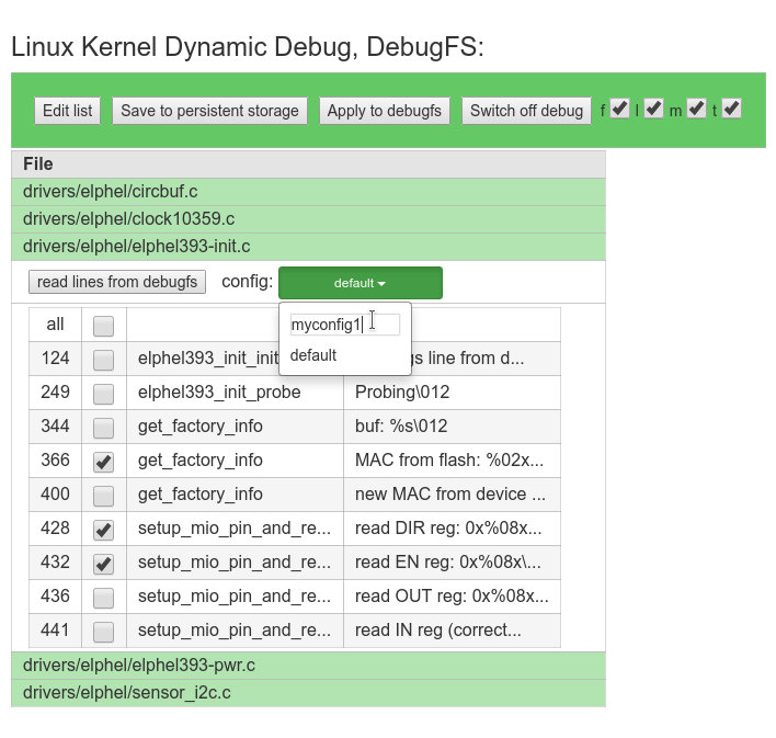
Fig.1 debugfs-webgui
In most cases it all works fine – when writing a linux driver you:
1. insert pr_debug()/dev_dbg() for debug messaging.
2. compile kernel with dyndbg enabled (CONFIG_DYNAMIC_DEBUG=y)
3. then just ‘echo‘ query strings or ‘cat‘ files with commands to switch on/off the debug messages at runtime. Examples:
- single:
echo -c 'file svcsock.c line 1603 +pfmt' > /dynamic_debug/control
- batch file:
cat query-batch-file > /dynamic_debug/control
When it’s all small – enabling/disabling the whole file or a function is not a problem. When the driver grows big with lots of debug messages or there are a few drivers interact with each other it becomes more convenient to have multiple configurations with certain debug lines on or off. As the source code changes the lines get shifted – and so, the batch files require editing.
If the target system (embedded or not) has network and a web browser (Apache2 + PHP) a quite simple solution is to add a web interface to the dynamic debug. The one we have developed has the following features:
- allows having multiple configurations for each file
- displays only files of interest
- updates debug configuration for modified files where debug lines got shifted
- keeps/updates the current config (in json format) in tmpfs – saves to disk on button click
- p, f, l, m, t flags are supported
Get the source code then proceed with the README.md.
I will not have to learn SystemVerilog
Or at least larger (verification) part of it – interfaces, packages and a few other synthesizable features are very useful to reduce size of Verilog code and make it easier to maintain. We now are able to run production target system Python code with Cocotb simulation over BSD sockets.
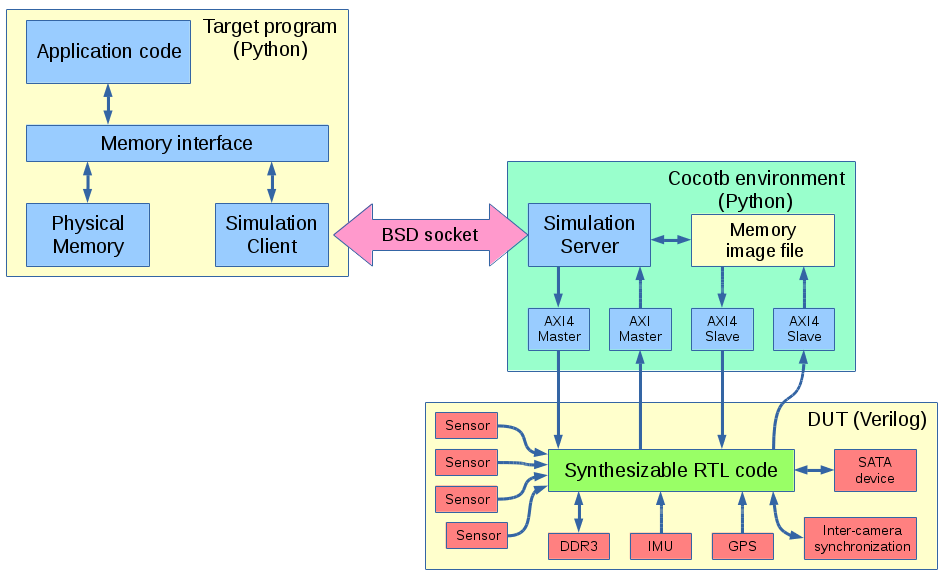
Client-server simulation of NC393 with Cocotb
Previous workflow
Before switching to Cocotb our FPGA-related workflow involved:
- Creating RTL design code
- Writing Verilog tests
- Running simulations
- Synthesizing and creating bitfile
- Re-writing test code to run on the target system in Python
- Developing kernel drivers to support the FPGA functionality
- Developing applications that access FPGA functionality through the kernel drivers
Of course the steps are not that linear, there are hundreds of loops between steps 1 and 3 (editing RTL source after finding errors at step 3), almost as many from 5 to 1 (when the problems reveal themselves during hardware testing) but few are noticed only at step 6 or 7. Steps 2, 5, 6+7 involve a gross violation of DRY principle, especially the first two. The last steps sufficiently differ from step 5 as their purpose is different – while Python tests are made to reveal the potential problems including infrequent conditions, drivers only use a subset of functionality and try to “hide” problems – perform recovering actions to maintain operation of the device after abnormal condition occurs.
We already tried to mitigate these problems – significant part of the design flexibility is achieved through parametrized modules. Parameters are used to define register map and register bit fields – they are one of the most frequently modified when new functionality is added. Python code in the camera is able to read and process Verilog parameters include files when running on the target system, and while generating C header files for the kernel drivers, so here DRY principle stands. Changes in any parameters definitions in Verilog files will be automatically propagated to both Python and C code.
But it is definitely not enough. Steps 2 and 5 may involve tens of thousands lines of code and large part of the Python code is virtually a literal translation from the Verilog original. All our FPGA-based systems (and likely it is true for most other applications) involve symbiotic operation of the FPGA and some general purpose processor. In Xilinx Zynq they are on the same chip, in our earlier designs they were connected on the PCB. Most of the volume of the Verilog test code is the simulation of the CPU running some code. This code interacts with the rest of the design through the writes/reads of the memory-mapped control/status registers as well as the system memory when FPGA is a master sending/receiving data over DMA.
This is one of the reasons I hesitated to learn verification functionality of SystemVerilog. There are tons of computer programming languages that may be a better fit to simulate program activity of the CPU (this is what they do naturally). Currently most convenient for bringing the new hardware to life seems to be Python, so I was interested in trying Cocotb. If I new it is that easy I would probably start earlier, but having rather large volume of the existing Verilog code for testing I was postponing the switch.
Trying CocotbTwo weeks ago I gave it a try. First I prepared the instruments – integrated Cocotb into VDT, made sure that Eclipse console output is clickable for the simulator reported problems, simulator output as well as for the errors in Python code and the source links in Cocotb logs. I used the Cocotb version of the JPEG encoder that has the Python code for simulation – just added configuration options for VDT and fixed the code to reduce number of warning markers that VDT generated. Here is the version that can be imported as Eclipse+VDT project.
Converting x393 camera project to Cocotb simulationNext was to convert simulation of our x393 camera project to use Cocotb. For that I was looking not just to replace Verilog test code with Python, but to use the same Python program that we already have running on the target hardware for simulation. The program already had a “dry run” option for development on a host computer, that part had to be modified to access simulator. I needed some way to effectively isolate the Python code that is linked to the simulator and the code of the target system, and BSD sockets provide a good match that. One part of the program that uses Cocotb modules and is subject to special requirement to the Python coroutines to work for simulation – it plays a role of the server. The other part (linked to the target system program) replaces memory accesses, sends the request parameters over the socket connection, and waits for the response from the server. The only other than memory access commands that are currently implemented are “finish” (to complete simulation and analyze the results in wave viewer – GtkWave), “flush” (flush file writes – similar to cache flushes on a real hardware) and interruptible (by the simulated system interrupt outputs) wait for specified time. Simulation time is frozen between requests from the client, so the target system has to specifically let the simulated system run for certain time (or until it will generate an interrupt).
Simulation clientBelow is the example of modification to the target code memory write (full source). X393_CLIENT is True: branch is for old dry run (NOP) mode, second one (elif not X393_CLIENT is None:) is for the simulation server and the last one accesses real memory over /dev/mem.
def write_mem (self,addr, data,quiet=1): """ Write 32-bit word to physical memory @param addr - physical byte address @param data - 32-bit data to write @param quiet - reduce output """ if X393_CLIENT is True: print ("simulated: write_mem(0x%x,0x%x)"%(addr,data)) return elif not X393_CLIENT is None: if quiet < 1: print ("remote: write_mem(0x%x,0x%x)"%(addr,data)) X393_CLIENT.write(addr, [data]) if quiet < 1: print ("remote: write_mem done" ) return with open("/dev/mem", "r+b") as f: page_addr=addr & (~(self.PAGE_SIZE-1)) page_offs=addr-page_addr mm = self.wrap_mm(f, page_addr) packedData=struct.pack(self.ENDIAN+"L",data) d=struct.unpack(self.ENDIAN+"L",packedData)[0] mm[page_offs:page_offs+4]=packedData if quiet <2: print ("0x%08x <== 0x%08x (%d)"%(addr,d,d))There is not much magic in initializing X393_CLIENT class instance:
print("Creating X393_CLIENT") try: X393_CLIENT= x393Client(host=dry_mode.split(":")[0], port=int(dry_mode.split(":")[1])) print("Created X393_CLIENT") except: X393_CLIENT= True print("Failed to create X393_CLIENT")And all the sockets handling code is less than 100 lines (source):
import json import socket class SocketCommand(): command=None arguments=None def __init__(self, command=None, arguments=None): # , debug=False): self.command = command self.arguments=arguments def getCommand(self): return self.command def getArgs(self): return self.arguments def getStart(self): return self.command == "start" def getStop(self): return self.command == "stop" def getWrite(self): return self.arguments if self.command == "write" else None def getWait(self): return self.arguments if self.command == "wait" else None def getFlush(self): return self.command == "flush" def getRead(self): return self.arguments if self.command == "read" else None def setStart(self): self.command = "start" def setStop(self): self.command = "stop" def setWrite(self,arguments): self.command = "write" self.arguments=arguments def setWait(self,arguments): # wait irq mask, timeout (ns) self.command = "wait" self.arguments=arguments def setFlush(self): #flush memory file (use when sync_for_* self.command = "flush" def setRead(self,arguments): self.command = "read" self.arguments=arguments def toJSON(self,val=None): if val is None: return json.dumps({"cmd":self.command,"args":self.arguments}) else: return json.dumps(val) def fromJSON(self,jstr): d=json.loads(jstr) try: self.command=d['cmd'] except: self.command=None try: self.arguments=d['args'] except: self.arguments=None class x393Client(): def __init__(self, host='localhost', port=7777): self.PORT = port self.HOST = host # Symbolic name meaning all available interfaces self.cmd= SocketCommand() def communicate(self, snd_str): sock = socket.socket(socket.AF_INET, socket.SOCK_STREAM) sock.connect((self.HOST, self.PORT)) sock.send(snd_str) reply = sock.recv(16384) # limit reply to 16K sock.close() return reply def start(self): self.cmd.setStart() print("start->",self.communicate(self.cmd.toJSON())) def stop(self): self.cmd.setStop() print("stop->",self.communicate(self.cmd.toJSON())) def write(self, address, data): self.cmd.setWrite([address,data]) rslt = self.communicate(self.cmd.toJSON()) def waitIrq(self, irqMask,wait_ns): self.cmd.setWait([irqMask,wait_ns]) rslt = self.communicate(self.cmd.toJSON()) def flush(self): self.cmd.setFlush() def read(self, address): self.cmd.setRead(address) rslt = self.communicate(self.cmd.toJSON()) return json.loads(rslt) Simulation serverServer code is larger (it now has 360 lines) but it is rather simple too. It runs in the Cocotb environment (coroutines that yield to simulator have “@cocotb.coroutine” decorations), receives and responds to the commands over the socket. When the command involves writing, it compares requested address to the pre-defined ranges and either sends data over one of the master AXI channels (defined in x393interfaces.py) or writes to the “system memory” – just a file system file with appropriate offset corresponding to the specified address)
elif self.cmd.getWrite(): ad = self.cmd.getWrite() self.dut._log.debug('Received WRITE, 0x%0x: %s'%(ad[0],hex_list(ad[1]))) if ad[0]in self.RESERVED: if ad[0] == self.INTM_ADDRESS: self.int_mask = ad[1][0] rslt = 0 elif (ad[0] >= self.memlow) and (ad[0] < self.memhigh): addr = ad[0] self._memfile.seek(addr) for data in ad[1]: # currently only single word is supported sdata=struct.pack(" 0x%08x"%(data,addr)) addr += 4 rslt = 0 elif(ad[0] >= 0x40000000) and (ad[0] < 0x80000000): rslt = yield self.maxigp0.axi_write(address = ad[0], value = ad[1], byte_enable = None, id = self.writeID, dsize = 2, burst = 1, address_latency = 0, data_latency = 0) self.dut._log.debug('maxigp0.axi_write yielded %s'%(str(rslt))) self.writeID = (self.writeID+1) & self.writeIDMask elif (ad[0] >= 0xc0000000) and (ad[0] < 0xfffffffc): self.ps_sbus.write_reg(ad[0],ad[1][0]) rslt = 0 else: self.dut._log.info('Write address 0x%08x is outside of maxgp0, not yet supported'%(ad[0])) rslt = 0 self.dut._log.info('WRITE 0x%08x <= %s'%(ad[0],hex_list(ad[1], max_items = 4))) self.soc_conn.send(self.cmd.toJSON(rslt)+"\n") self.dut._log.debug('Sent rslt to the socket')Similarly read commands acquire data from either AXI read channel or from the same memory image file. Data is sent to this file over the AXI slave interface by the simulated device.
Top Verilog moduleThe remaining part of the conversion form plain Verilog to Cocotb simulation is the top Verilog file – x393_dut.v. It contains an instance of the actual synthesized module (x393_i) and Verilog simulation modules of the connected peripherals. These modules can also be replaced by Python ones (and some eventually will be), but others, like Micron DDR3 memory model, are easier to use as they are provided by the chip manufacturer.
Python modules can access hierarchical nodes in the design, but to keep things cleaner all the design inputs and outputs are routed to/from the outputs/inputs of the x393_dut module. In the case of Xilinx Zynq that involves connecting internal nodes – Zynq considers CPU interface not as I/O, but as an empty module (PS7) instantiated in the design.
Screenshot of the simulation with client (black console) and server (in Eclipse IDE)
Conclusions
Conversion to Python simulation was simple, considering rather large amount of project (Python+Verilog) code – about 100K lines. After preparing the tools it took just one week and now we have the same code running both on the real hardware and in the simulator.
Splitting the simulation into client/server duo makes it easy to use any other programming language on the client side – not just the Python of our choice. Unix sockets provide convenient means for that. Address decoder (which decides what interface to use for the received memory access request) is better to keep on the server (simulator) side of the socket connection, not on the client. This minimizes changes to the target code and the server is playing the role of the memory-mapped system bus, behaves as the real hardware does.
Are there any performance penalties compared to all-Verilog simulation? None visible in our designs. Simulation (and Icarus Verilog is a single-threaded application) is the most time-consuming part – for our application it is about 8,000,000 times slower than the modeled hardware. Useful simulations (all-Verilog) for the camera runs for 15-40 minutes with tiny 64×32 pixel images. If we ran normal set of 14 MPix frames it would take about a week for the first images to appear at the output. Same Python code on the target runs for a fraction of a second, so even as the simulator is stopped while Python runs, combined execution time does not noticeably change for the Python+Verilog vs. all-Verilog mode. It would be nice to try to use Verilator in addition to Icarus. While it is not a real Verilog simulator (it can not handle ‘bx and ‘bz values, just ‘0’ and ‘1’) it is much faster.
Tutorial 02: Eclipse-based FPGA development environment for Elphel cameras
Elphel cameras offer unique capabilities – they are high performance systems out of the box and have all the firmware and FPGA code distributed under GNU General Public Licenses making it possible for users to modify any part of the code. The project does not use any “black boxes” or encrypted modules, so it is simulated with the free software tools and user has access to every net in the design. We are trying to do our best to make this ‘hackability’ not just a theoretical possibility, but a practical one.
Current camera FPGA project contains over 400 files under version control and almost 100K lines of HDL (Verilog) code, there are also constraints files, tool configurations, so we need to provide means for convenient navigation and modification of the project by the users.
We are starting a series of tutorials to facilitate acquaintance with this project, and here is the first one that shows how to install and configure the software. This tutorial is made with a fresh Kubuntu 16.04 LTS distribution installed on a virtual machine – this flavor of GNU/Linux we use ourselves and so it is easier for us to help others in the case of problems, but it should be also easy to install it on other GNU/Linux systems.
Later we plan to show how to navigate code and view/modify tool parameters with VDT plugin, run simulation and implementation tools. Next will be a “Hello world” module added to the camera code base, then some simple module that accesses the video memory.
Video resolution is 1600×900 pixels, so full screen view is recommended.
Download links for: video and captions.
Running this software does not require to have an actual camera, so it may help our potential users to evaluate software capabilities and see if it matches their requirements before purchasing an actual hardware. We will also be able to provide remote access to the cameras in our office for experimenting with them.
3D Print Your Camera Freedom
Two weeks ago we were making photos of our first production NC393 camera to post an announcement of the new product availability. We got all the mechanical parts and most of the electronic boards (14MPix version will be available shortly) and put them together. Nice looking camera, powered by a high performance SoC (dual ARM plus FPGA), packaged in a lightweight aluminum extrusion body, providing different options for various environments – indoors, outdoors, on board of the UAV or even in the open space with no air (cooling is important when you run most of the FPGA resources at full speed). Tons of potential possibilities, but the finished camera did not seem too exciting – there are so many similar looking devices available.
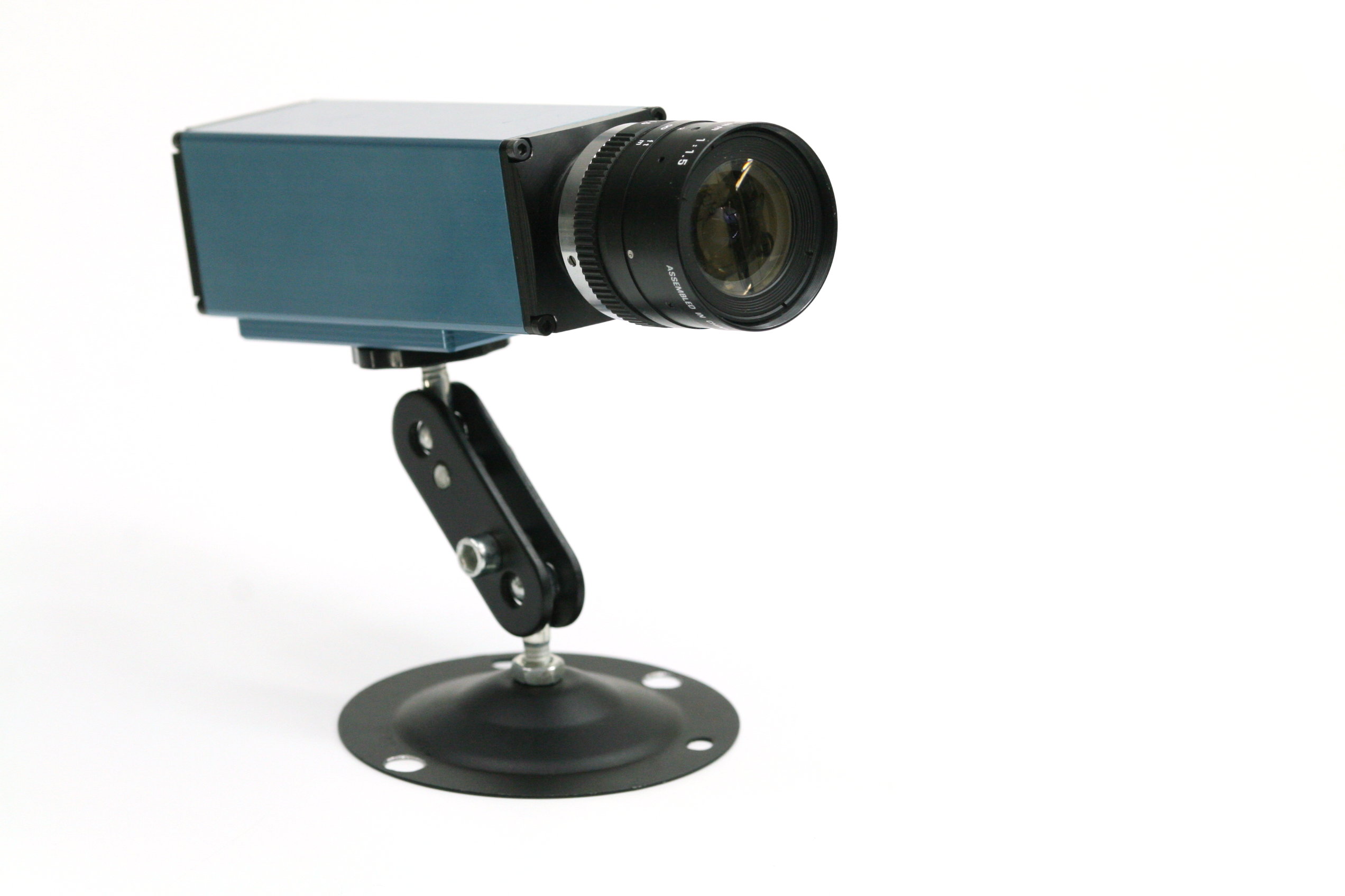
NC393 camera, front view
NC393 camera, back panel view. Includes DC power input (12-36V and 20-75V options), GigE, microSD card (bootable), microUSB(type B) connector for a system console with reset and boot source selection, USB/eSATA combo connector, microUSB(type A) and 2.5mm 4-contact barrel connector for external synchronization I/O
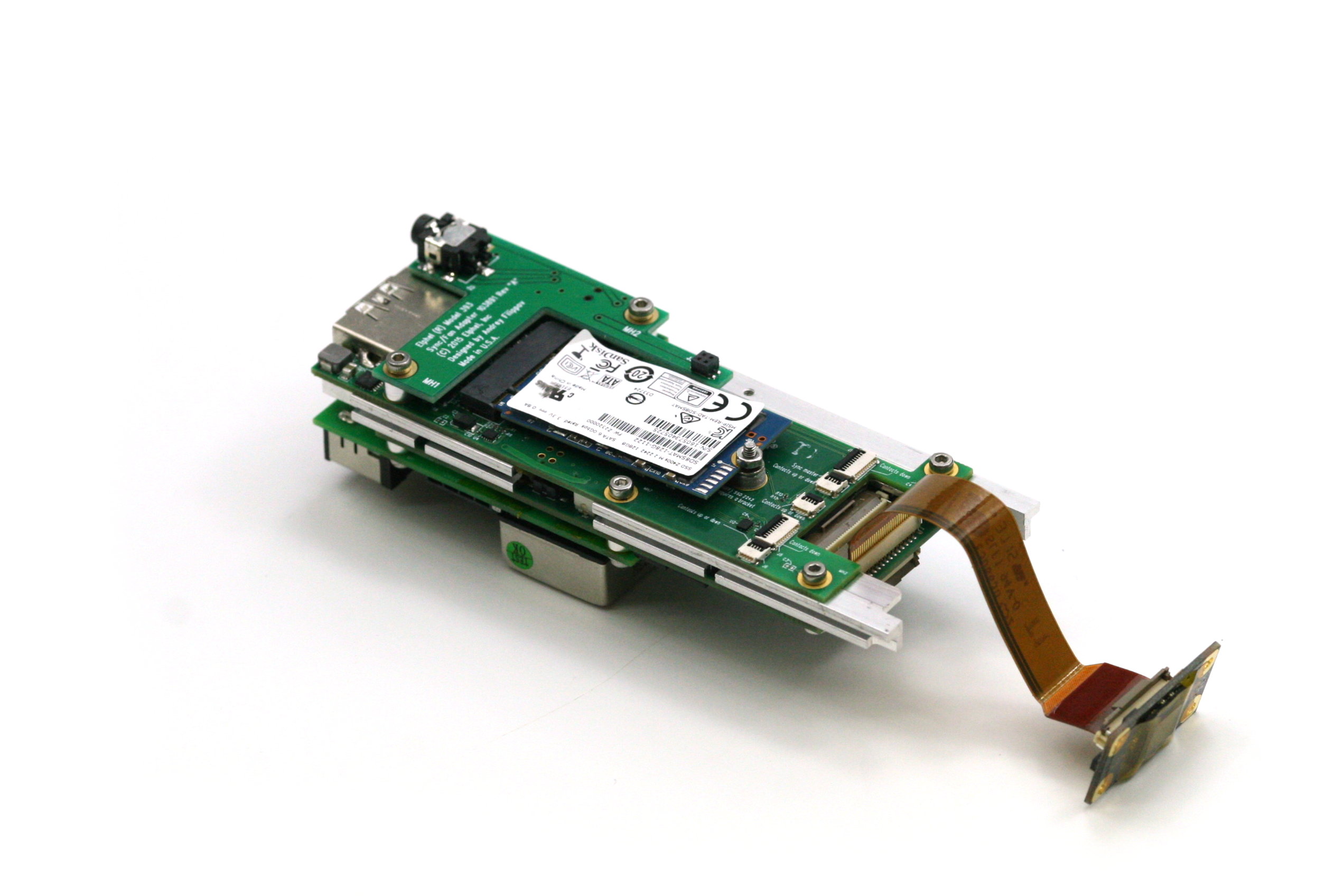
NC393 assembled boards: 10393(system board), 10385 (power supply board), 10389(interface board), 10338e (sensor board) and 103891 - synchronization adapter board, view from 10389. m.2 2242 SSD shown, bracket for the 2260 format provided. 10389 internal connectors include inter-camera synchronization and two of 3.3VDC+5.0VDC+I2C+USB ones.
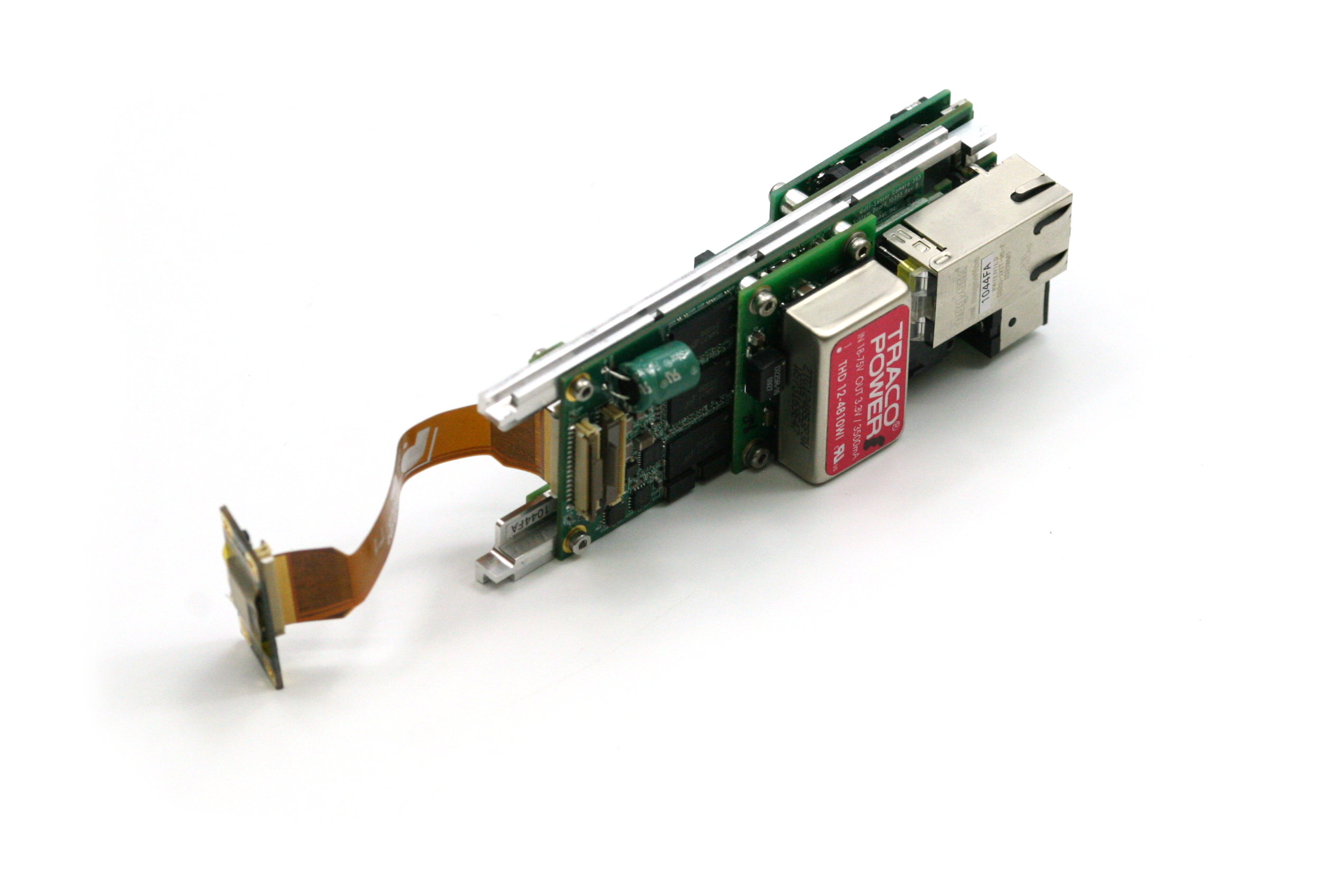
NC393 assembled boards: 10393(system board), 10385 (power supply board), 10389(interface board), 10338e (sensor board) and 103891 - synchronization adapter board, view from 10385
10393 system board attached to the heat frame, view from the heat frame. There is a large aluminum heat spreader attached to the other side of the frame with thermal conductive epoxy that provides heat transfer from the CPU without the use of any spring load. Other heat dissipating components use heat pads.
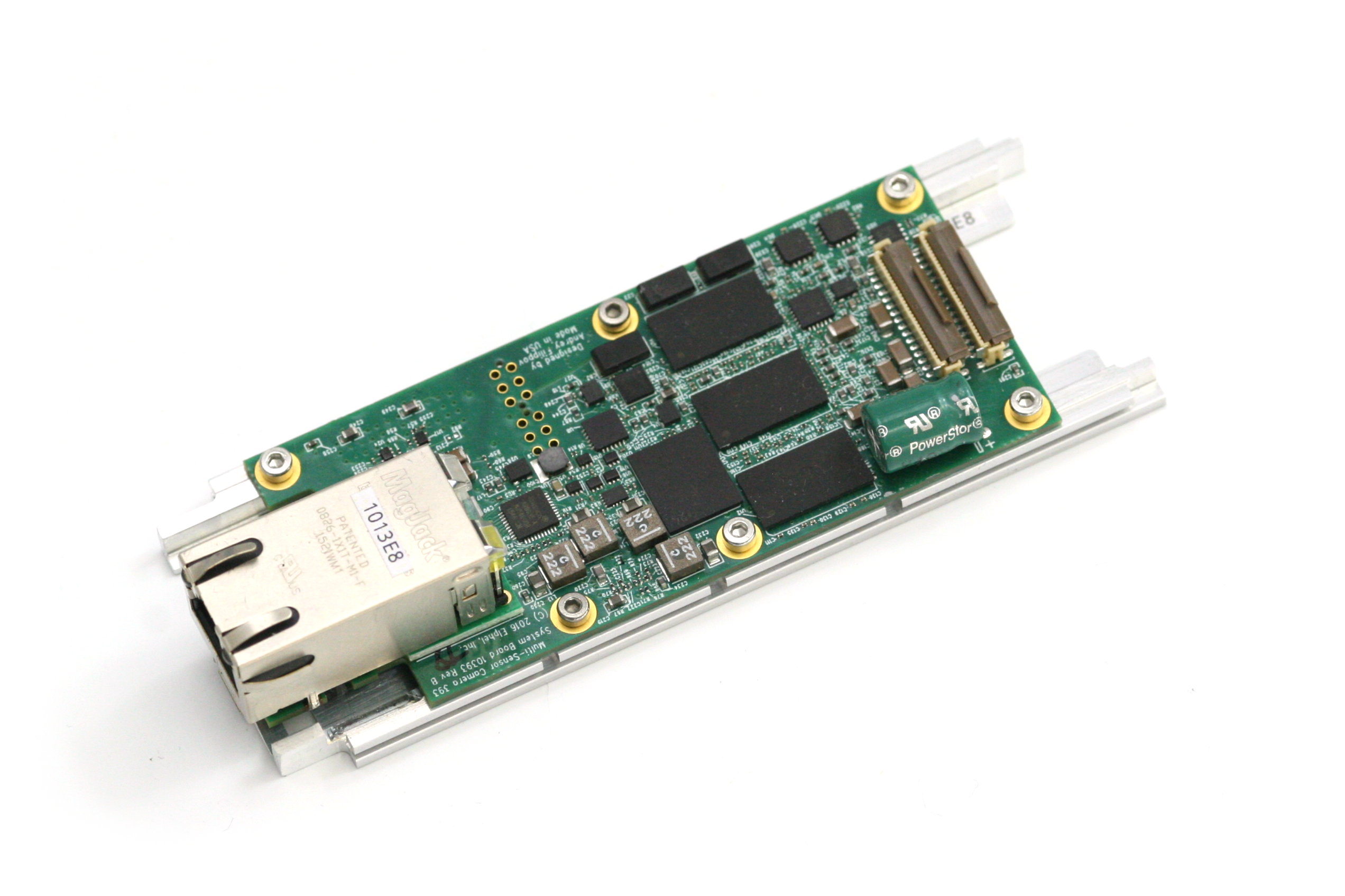
10393 system board attached to the heat frame, view from the 10393 board
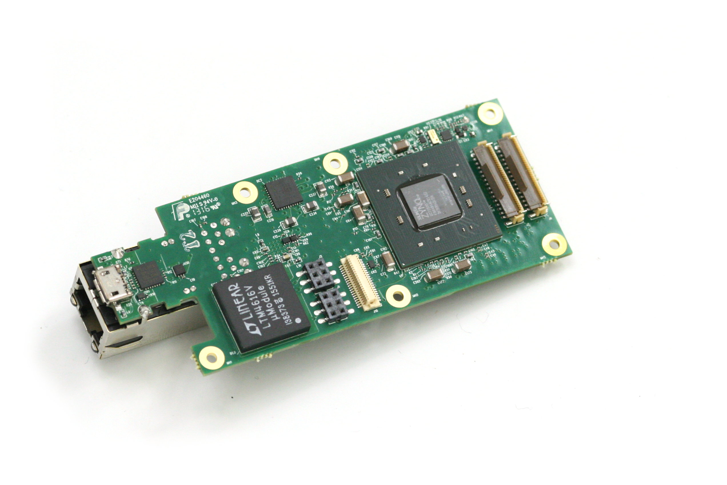
10393 system board, view from the processor side
(function ( $ ) { "use strict"; $(function () { var masterslider_eceb = new MasterSlider(); // slider controls masterslider_eceb.control('arrows' ,{ autohide:true, overVideo:true }); masterslider_eceb.control('thumblist' ,{ autohide:false, overVideo:true, dir:'h', speed:17, inset:false, arrows:false, hover:false, customClass:'', align:'bottom',type:'thumbs', margin:10, width:100, height:80, space:5, fillMode:'fill' }); masterslider_eceb.control('slideinfo' ,{ autohide:false, overVideo:true, dir:'h', align:'bottom',inset:false , margin:10 , size:60 }); // slider setup masterslider_eceb.setup("MS57323cfcaeceb", { width : 800, height : 480, minHeight : 0, space : 0, start : 1, grabCursor : true, swipe : true, mouse : true, layout : "boxed", wheel : false, autoplay : false, instantStartLayers:false, loop : true, shuffle : false, preload : 0, heightLimit : true, autoHeight : false, smoothHeight : true, endPause : false, overPause : true, fillMode : "fill", centerControls : true, startOnAppear : false, layersMode : "center", hideLayers : false, fullscreenMargin: 0, speed : 20, dir : "h", parallaxMode : 'swipe', view : "basic" }); window.masterslider_instances = window.masterslider_instances || []; window.masterslider_instances.push( masterslider_eceb ); }); })(jQuery);An obvious reason for our dissatisfaction is that the single-sensor camera uses just one of four available sensor ports. Of course it is possible to use more of the freed FPGA resources for a single image processing, but it is not what you can use out of the box. Many of our users buy camera components and arrange them in their custom setup themselves – that does not have a single-sensor limitation and it matches our goals – make it easy to develop a custom system, or sculpture the camera to meet your ideas as stated on our web site. We would like to open the cameras to those who do not have capabilities of advanced mechanical design and manufacturing or just want to try new camera ideas immediately after receiving the product. Why multisensor?
One simple answer can be “because we can” – the CPU+FPGA based camera system can simultaneously handle multiple small image sensors we love – sensors perfected by the cellphone industry. Of course it is also possible to connect one large (high resolution/high FPS) sensor or even to use multiple camera system for one really fast sensor – we did such trick with the NC323 camera for book scanning, but we believe that the future is with the multiple view systems that combine images from several synchronized cameras using computational photography rather than large lens/large sensor traditional cameras.
Multi-sensor systems can acquire high-resolution panoramic images in a single shot (or offer full sphere live video), they can be used for image-based 3-d reconstruction that in many cases provide much superior quality to the now traditional LIDAR-based scanners which can not output cinematographic quality 3-d scenes. They can be used to capture HDR video by combining data for the same voxels rather than pixels. Such systems can easily beat the shallow depth of field of the traditional large format cameras and offer possibility of the post-production focus distance adjustment. Applications are virtually endless, and while at Elphel we are developing such multi-sensor systems our main products are still the high-performance camera systems hackable at any imaginable level.
Prototype of the 21-sensor 3D HDR 6K cinematographic camera
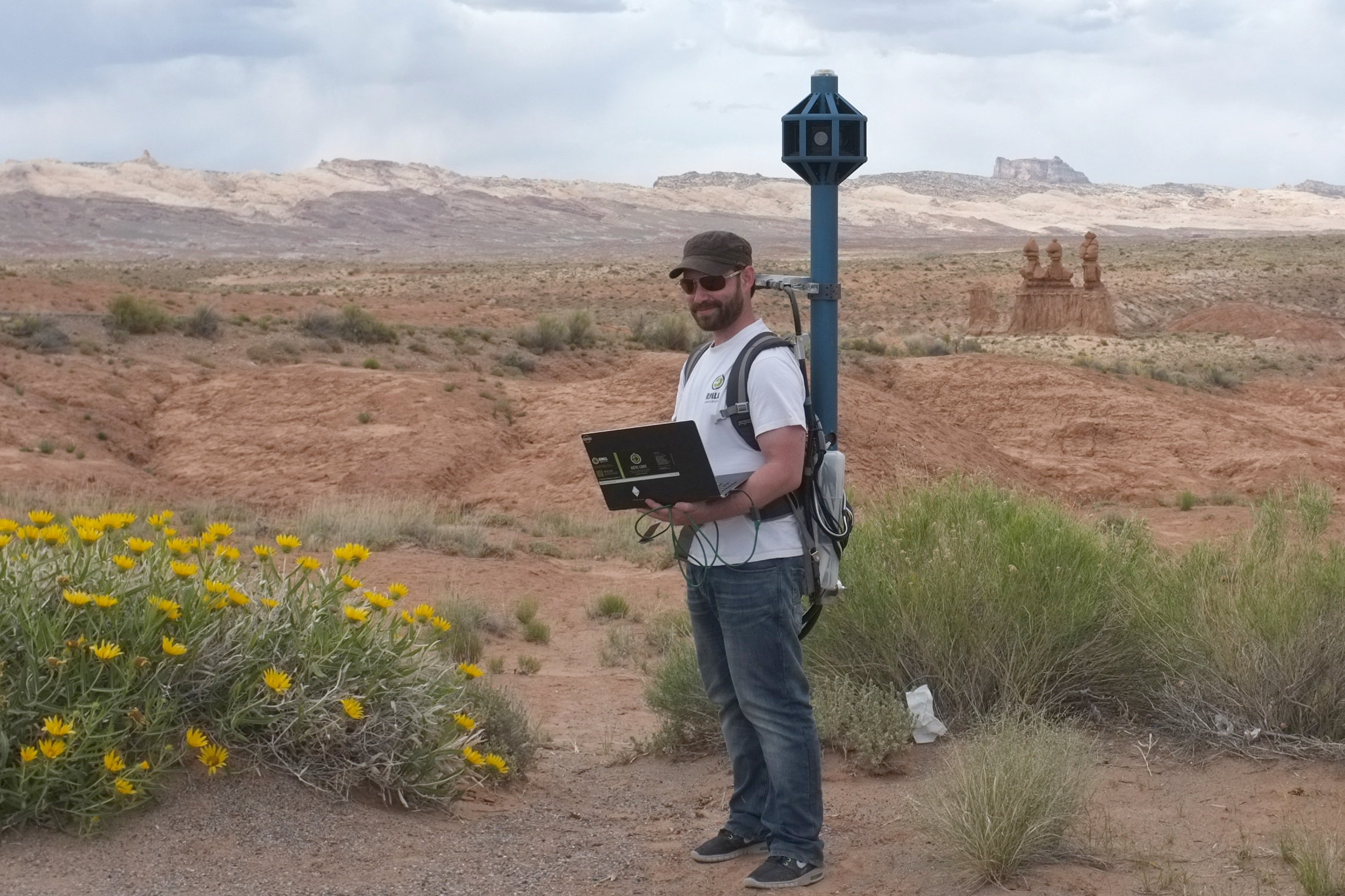
Eyesis4π stereophotogrammetric camera
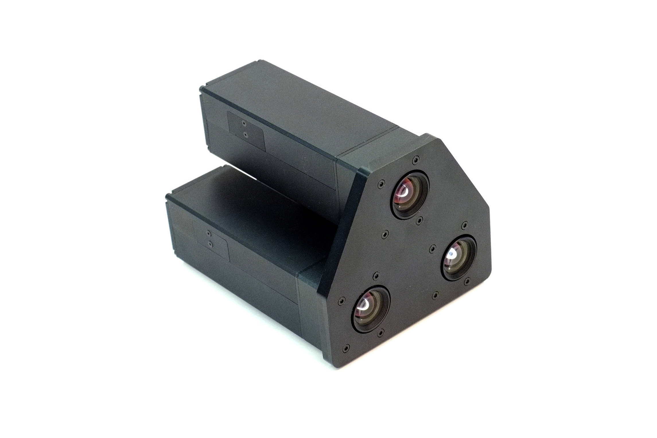
NC353-369-PHG3 3-sensor camera camera, view demo (mouse scroll changes disparity, shift-scroll - zoom)
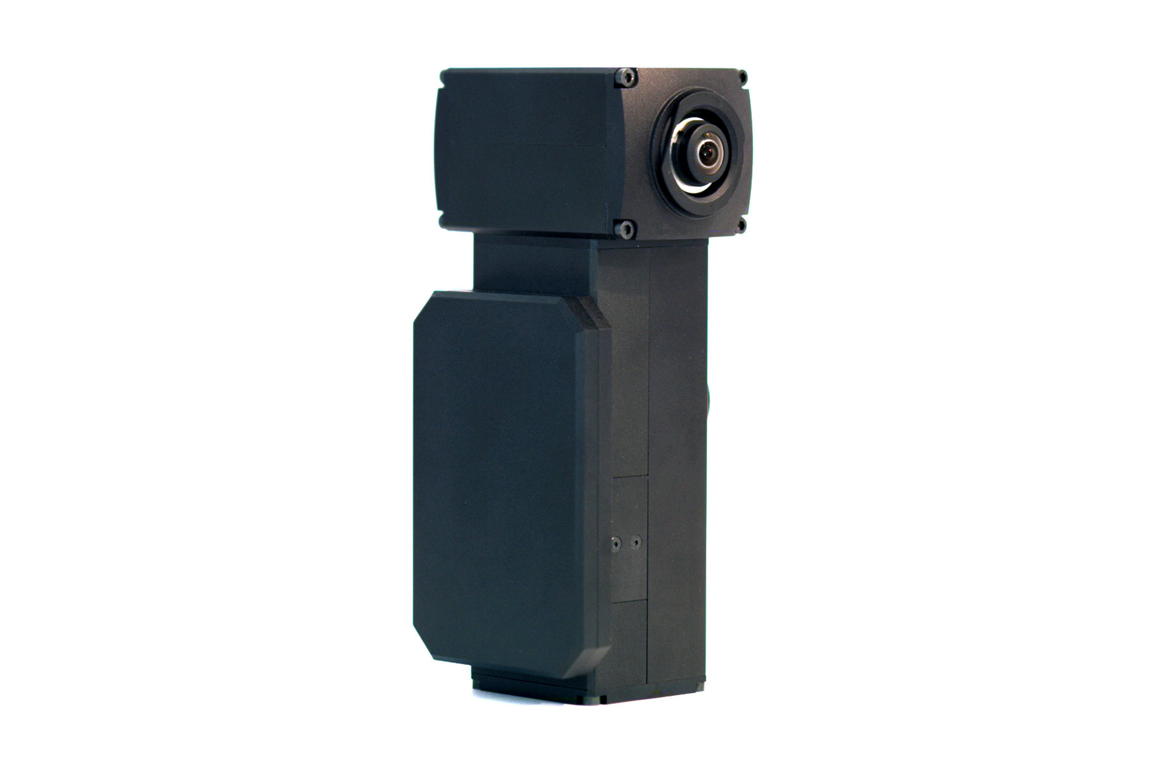
Spherical view camera with two fish eye lenses
Two sensor stereo camera with two interchangeable C/CS-mount lenses
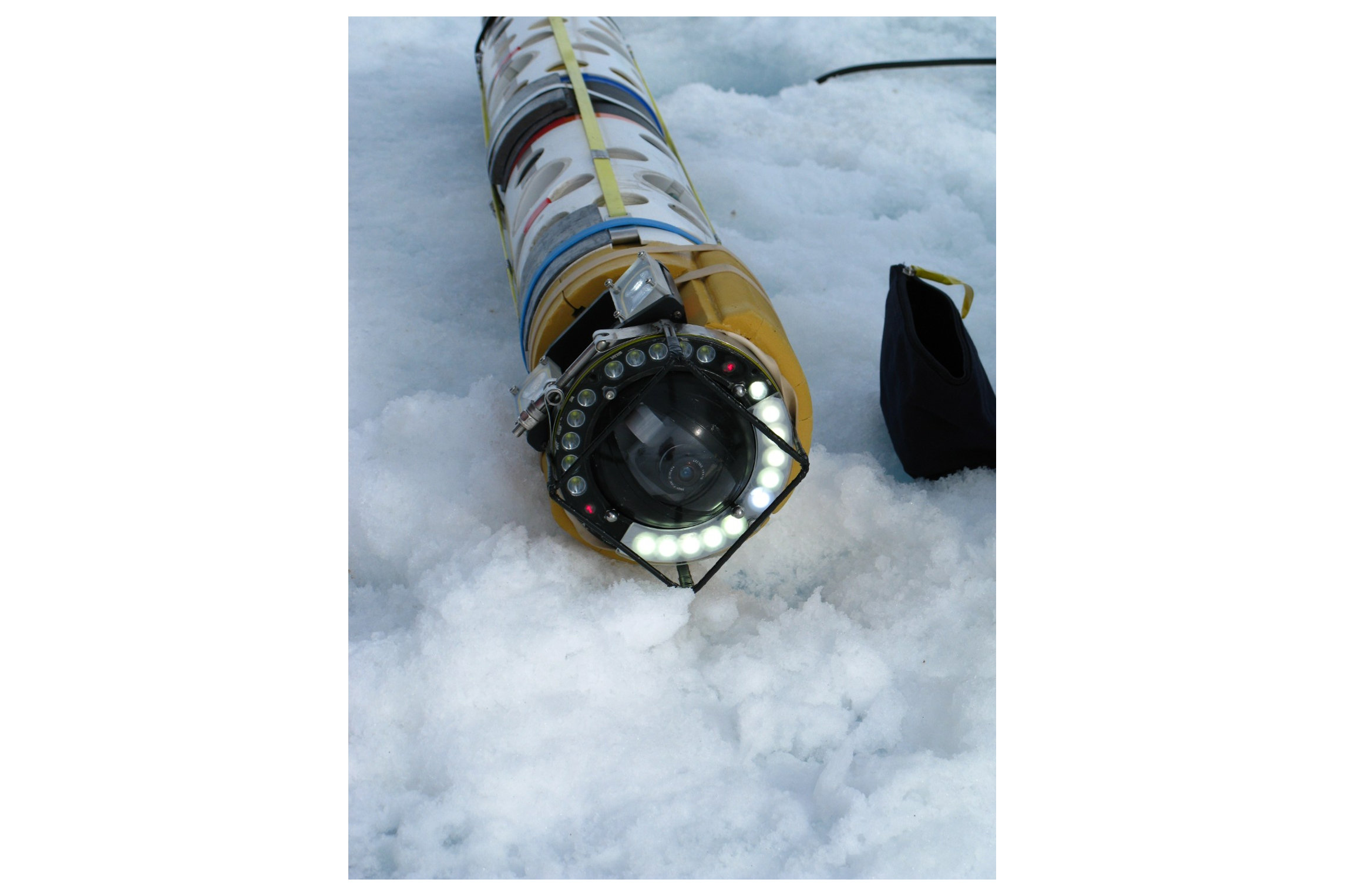
SCINI project underwater remotely operated vehicle (ROV)
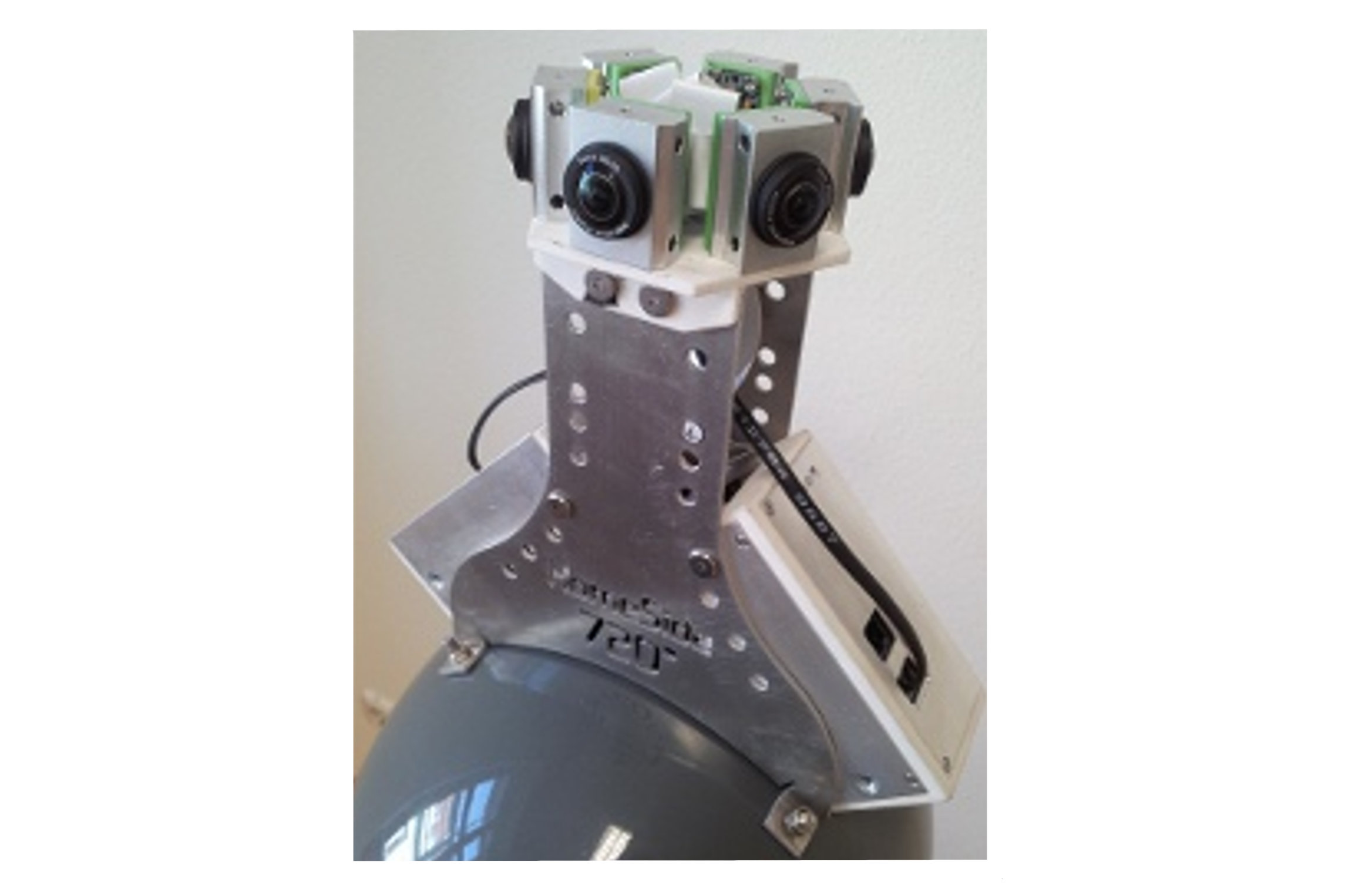
A helmet-mounted panoramic camera by HomeSide 720°
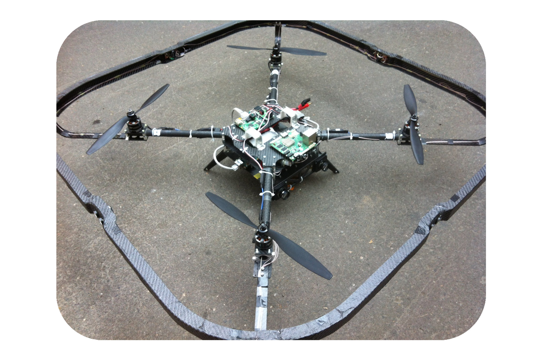
Quadcopter using multisensor camera for navigation, by 'Autonomous Aerospace' team in Krasnoyarsk, Russia
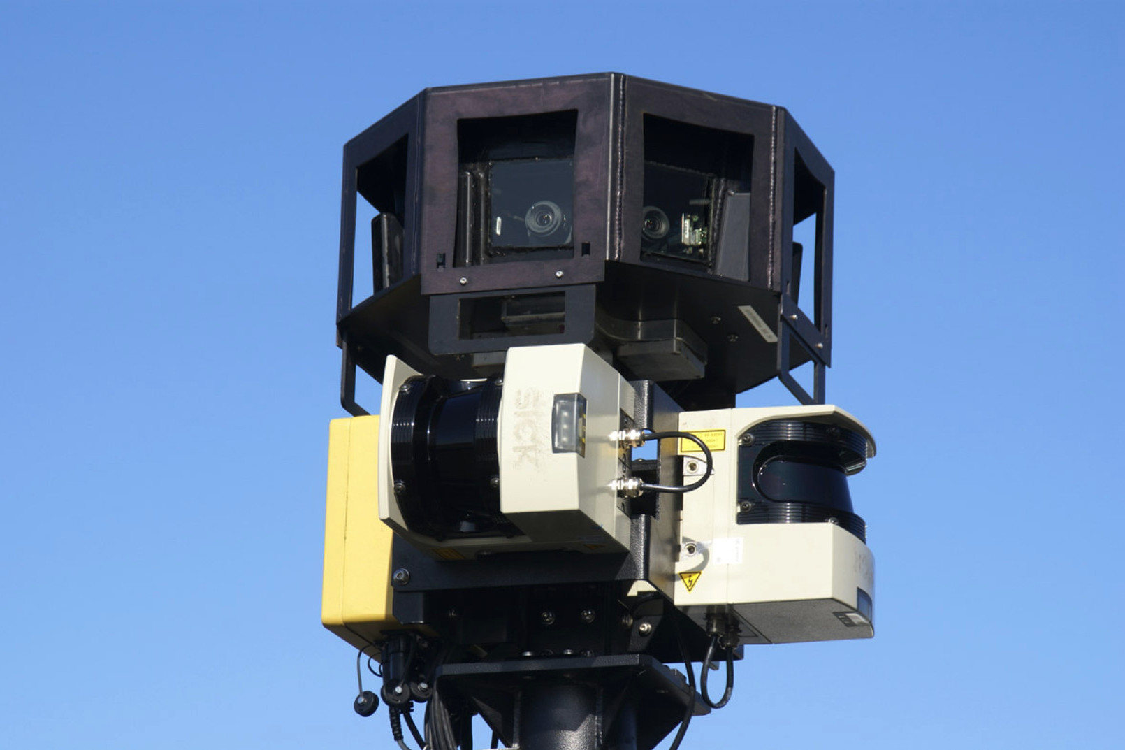
Multisensor R5 camera by Google
(function ( $ ) { "use strict"; $(function () { var masterslider_17e3 = new MasterSlider(); // slider controls masterslider_17e3.control('arrows' ,{ autohide:true, overVideo:true }); masterslider_17e3.control('thumblist' ,{ autohide:false, overVideo:true, dir:'h', speed:17, inset:false, arrows:false, hover:false, customClass:'', align:'bottom',type:'thumbs', margin:10, width:100, height:80, space:5, fillMode:'fill' }); masterslider_17e3.control('slideinfo' ,{ autohide:false, overVideo:true, dir:'h', align:'bottom',inset:false , margin:10 , size:40 }); // slider setup masterslider_17e3.setup("MS57323cfcb17e3", { width : 800, height : 480, minHeight : 0, space : 0, start : 1, grabCursor : true, swipe : true, mouse : true, layout : "boxed", wheel : false, autoplay : false, instantStartLayers:false, loop : true, shuffle : false, preload : 0, heightLimit : true, autoHeight : false, smoothHeight : true, endPause : false, overPause : true, fillMode : "fill", centerControls : true, startOnAppear : false, layersMode : "center", hideLayers : false, fullscreenMargin: 0, speed : 20, dir : "h", parallaxMode : 'swipe', view : "basic" }); window.masterslider_instances = window.masterslider_instances || []; window.masterslider_instances.push( masterslider_17e3 ); }); })(jQuery); Hackable by DesignTo have all documentation open and released under free licenses such as GNU GPL and CERN OHL is a precondition, but it is not sufficient. The hackable products must be designed to be used that way and we strive to provide this functionality to our users. This is true for the products themselves and for the required tools, so we had to go as far as to develop software for FPGA tools integration with the popular Eclipse IDE and replace closed source manufacturer code that is not compatible with the free software Verilog simulators.
Same is true for the camera mechanical parts – users need to be able to reconfigure not just the firmware, FPGA code or rearrange the electronic components, but to change the physical layout of their systems. One popular solution to this challenge is to offer modular camera systems, but unfortunately this approach has its limits. It is similar to Lego® sets (where kids can assemble just one object already designed by the manufacturer) vs. Lego® bricks where the possibilities are limited by the imagination only. Often camera modularity is more about marketing (suggesting that you can start with a basic less expensive set and later buy more parts) than about the real user freedom.
We too provide modular components and try to maintain compatibility between the generations of modules – new Elphel cameras can directly interface more than a decade old sensor boards and this does not prevent them from simultaneously supporting modern sensor interfaces. Physical dimensions and shapes of the camera electronic boards also remain the same – they just pack more performance in the same volume as newer components become available. Being in the business of developing hackable cameras for 15 years, we realize that the modularity alone is not a magic bullet. Luckily now there are other possibilities.
3d printing camera parts3d printing process offers freedom in the material world but so far we were pessimistic about its use for the camera components where microns often matter. Some of the camera modules use invar (metal alloy that has almost zero thermal expansion coefficient at normal temperatures) elements to compensate for the thermal expansion, and the PLA plastic parts seem rather alien here. Nevertheless it is possible to meet the requirements of the camera mechanical design even with this material. In some cases it is sufficient to have precise and stable sensor/lens combination – sensor front end (SFE), small fluctuations in the mutual position/orientation of the individual SFE may be compensated using image data itself in the overlapping areas. It is possible to design composite structure that combines metal elements of simple shape (such as aluminum, thin wall stainless steel tubes or even small diameter invar rods) and printed elements of complex shape. Modern fiber-reinforced material for 3d-printing promise to improve mechanical stability and reduce thermal expansion of the finished parts.
This technology perfectly fits to the hackable multi-sensor systems and fills important missing part of “sculpturing” the user camera. 3-d printing is slow and we can not print every camera, but that is not really needed. While we certainly can print some parts, we are counting that this technology is now available in most parts of the world where we ship the products, and the parts can be manufactured by the end user. We anticipate that many of the customer designs being experimental by nature will need later modifications, building the parts by the user can save on the overseas shipments too.
We count that the users will design their own parts, but we will try to make their job easier and provide modifiable design examples and fragments that can be used in their parts. This idea of incorporating 3-d printing technology into Elphel products is just 2 weeks old and we prepared several quick design prototypes to try it – below are some examples of our first generation of such camera parts.
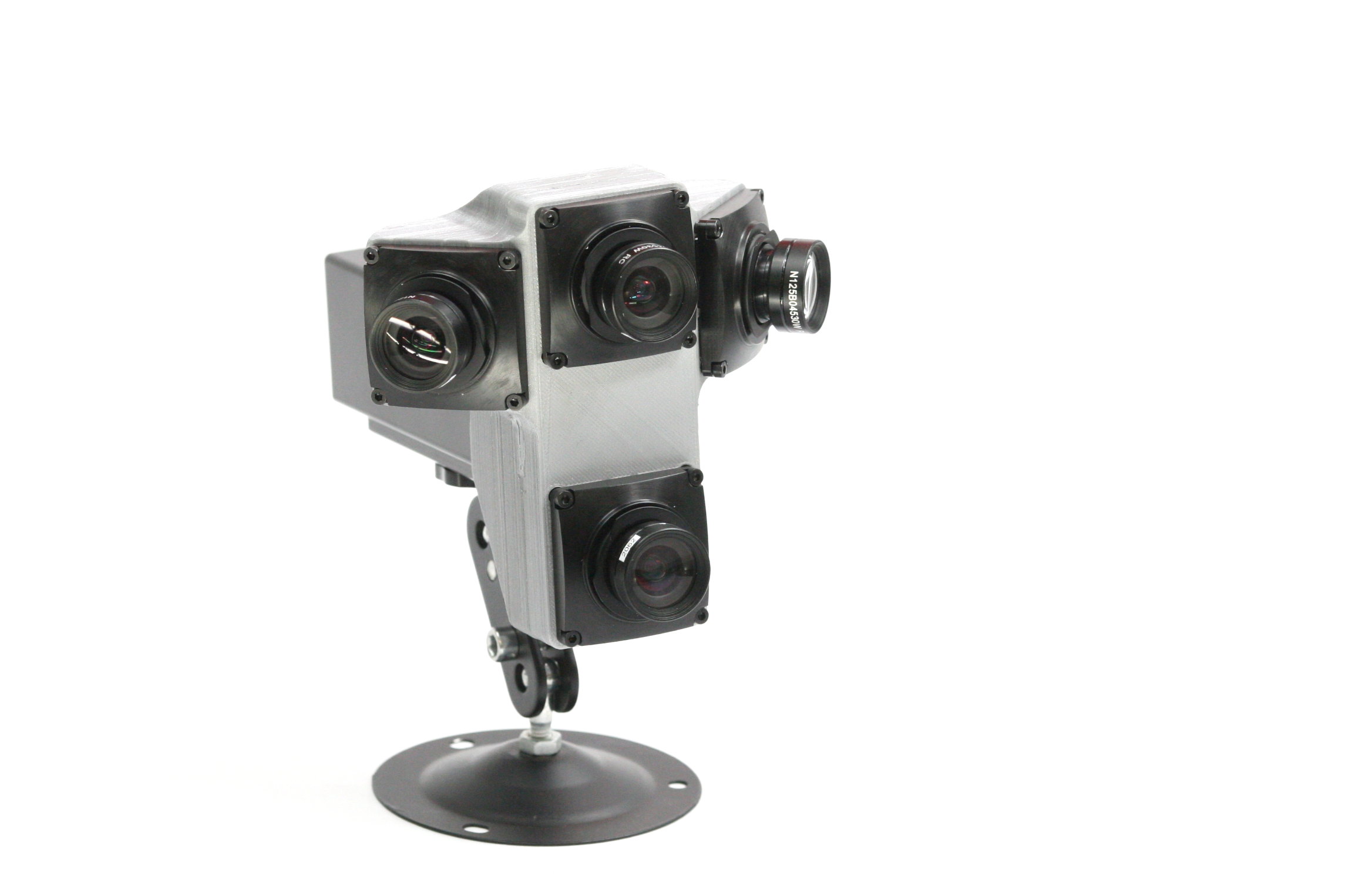
Panoramic camera with perfect stitching - it uses 2 center cameras to measure distances
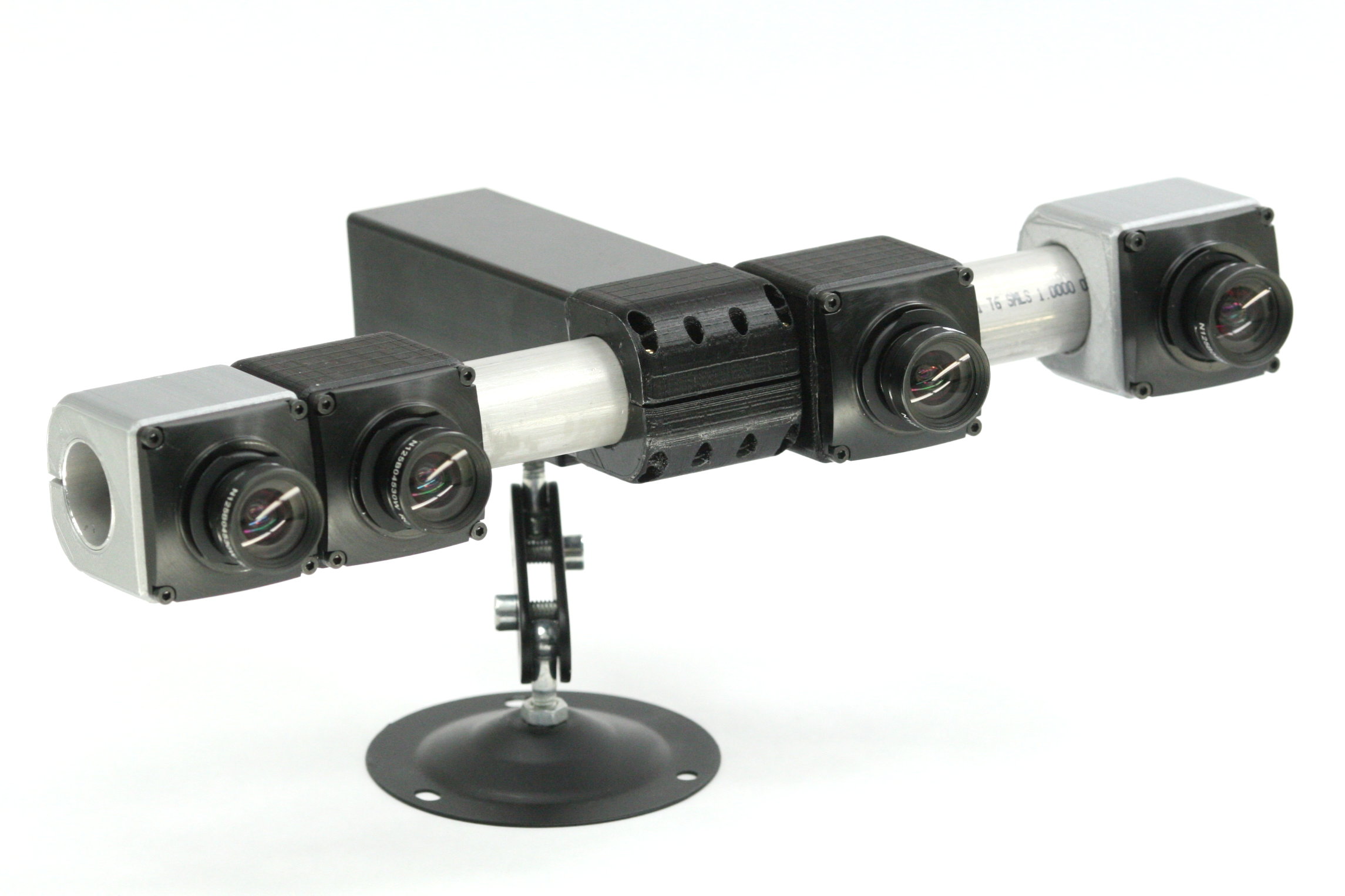
Stereo camera with 4 sensors having 1:3:2 bases providing all integer 1 to 6 multiples of 43mm in the lens pairs
Rectangular arranged 4-sensor stereo camera, adjustable bases
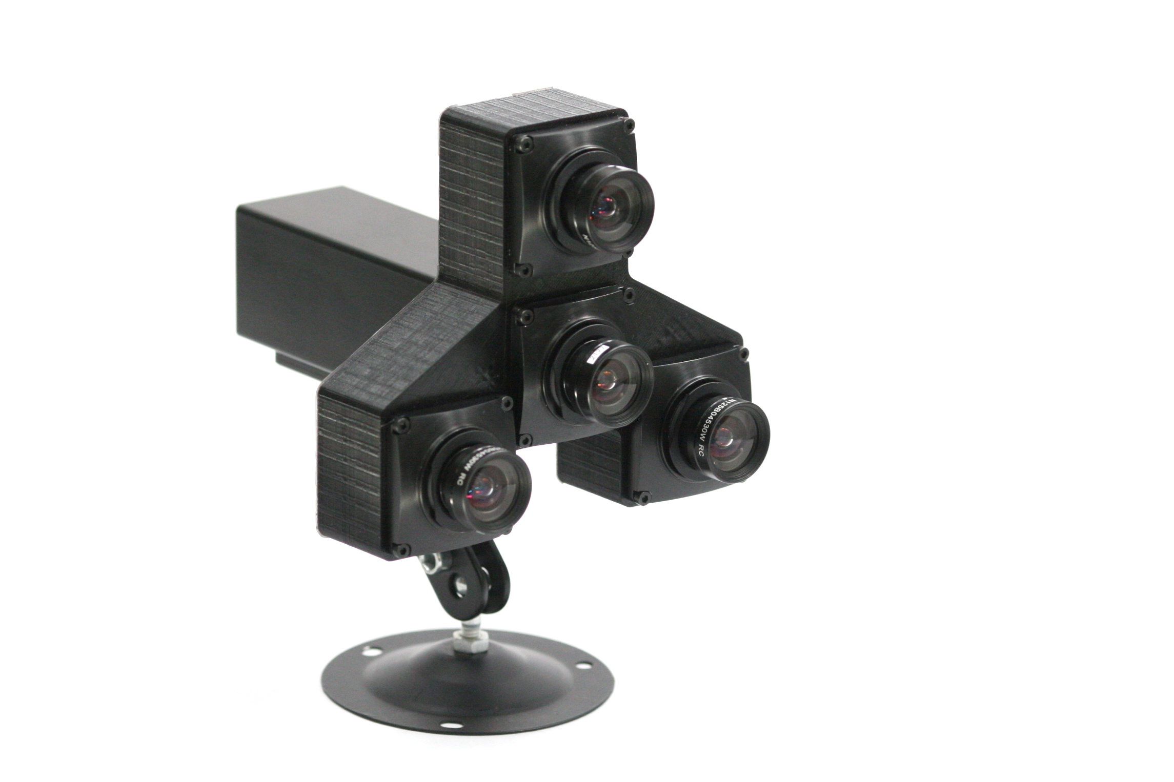
Short-base (48mm form center) 4-sensor camera
Printed adapter for the SFE of the 4-sensor panoramic camera
Printed adapter for the short-base 4-sensor camera
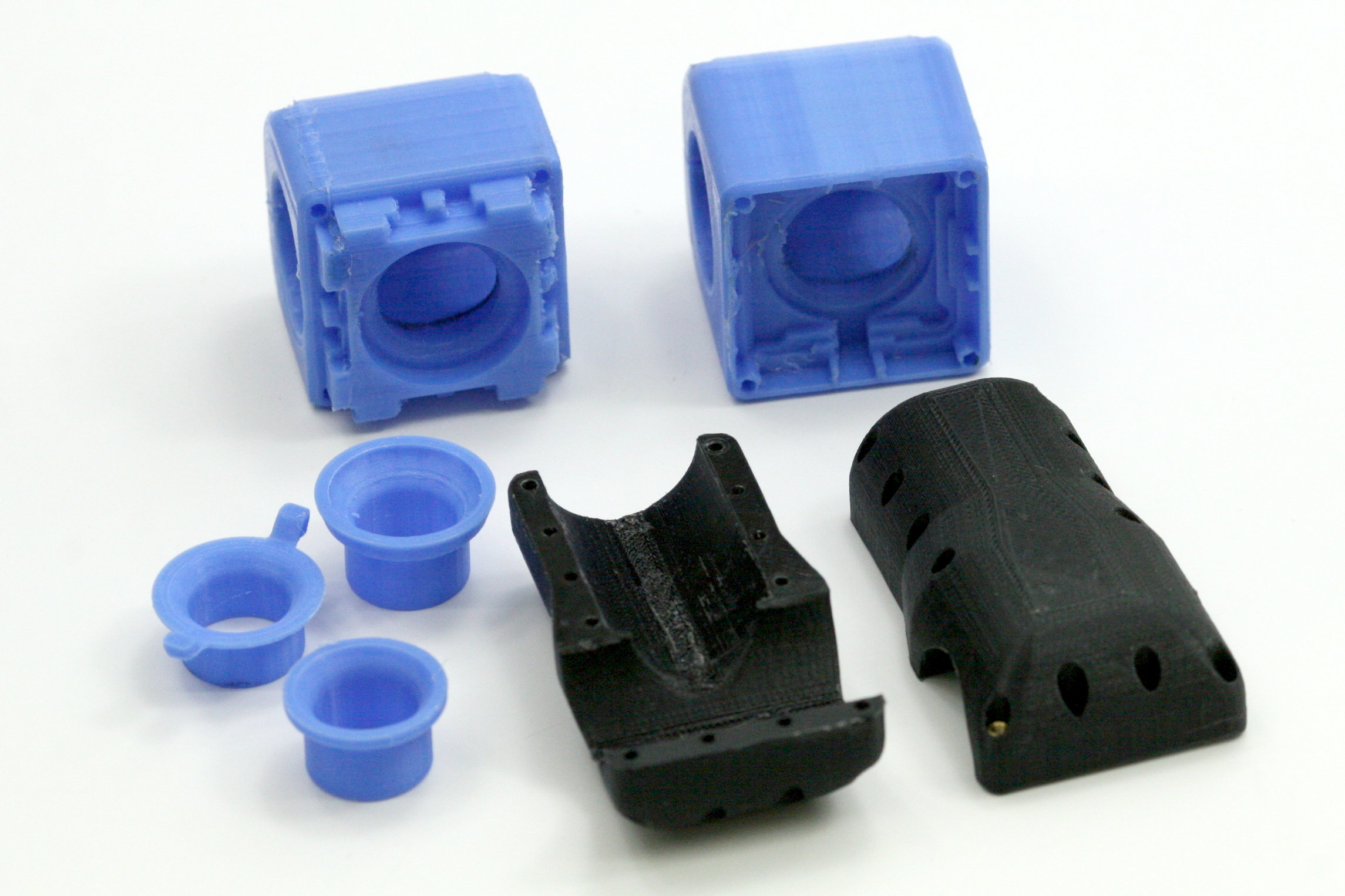
Various 3-d printed camera parts
It takes about 3 hours to print one SFE adapter
(function ( $ ) { "use strict"; $(function () { var masterslider_46c2 = new MasterSlider(); // slider controls masterslider_46c2.control('arrows' ,{ autohide:true, overVideo:true }); masterslider_46c2.control('thumblist' ,{ autohide:false, overVideo:true, dir:'h', speed:17, inset:false, arrows:false, hover:false, customClass:'', align:'bottom',type:'thumbs', margin:10, width:100, height:80, space:5, fillMode:'fill' }); masterslider_46c2.control('slideinfo' ,{ autohide:false, overVideo:true, dir:'h', align:'bottom',inset:false , margin:10 , size:40 }); // slider setup masterslider_46c2.setup("MS57323cfcb46c2", { width : 800, height : 480, minHeight : 0, space : 0, start : 1, grabCursor : true, swipe : true, mouse : true, layout : "boxed", wheel : false, autoplay : false, instantStartLayers:false, loop : true, shuffle : false, preload : 0, heightLimit : true, autoHeight : false, smoothHeight : true, endPause : false, overPause : true, fillMode : "fill", centerControls : true, startOnAppear : false, layersMode : "center", hideLayers : false, fullscreenMargin: 0, speed : 20, dir : "h", parallaxMode : 'swipe', view : "basic" }); window.masterslider_instances = window.masterslider_instances || []; window.masterslider_instances.push( masterslider_46c2 ); }); })(jQuery); Deliverables“3d print your camera freedom” – we really mean that. It is not about printing of a camera or its body. You can always get a complete camera in one of the available configurations packaged in a traditional all-metal body if it matches your ideas, printing just adds freedom to the mechanical design.
We will continue to provide all the spectrum of the camera components such as assembled boards and sensor front ends as well as the complete cameras in multiple configurations. For the 3-d printed versions we will have the models and reusable design fragments posted online. We will be able to print some parts and ship the factory assembled cameras. In some cases we may be able to help with the mechanical design, but we try to avoid doing any custom design ourselves. We consider our job is done well if we are not needed to modify anything for the end user. Currently we use one of the proprietary mechanical CAD programs so we do not have fully editable models and can only provide exported STEP files of the complete parts and interface fragments that can be incorporated in the user designs.
We would like to learn how to do this in FreeCAD – then it will be possible to provide the usable source files and detailed instructions how to customize them. FreeCAD environment can be used to create custom generator scripts in Python – this powerful feature helped us to convert all our mechanical design files into x3d models that can be viewed and navigated in the browser (video tutorial). This web based system proved to be not just a good presentation tool but to be more convenient for parts navigation than the CAD program itself, we use it ourselves regularly for that purpose.
Maybe we’ll be able to find somebody who is both experienced in mechanical design in FreeCAD and interested in multi-sensor camera systems to cooperate on this project?
Tutorial 01: Access to Elphel camera documentation from 3D model
We have created a short video tutorial to help our users navigate through 3D models of Elphel cameras. Cameras can be virtually taken apart and put back together which helps to understand the camera configuration and access information about every camera component. Please feel free to comment on the video quality and usefulness, as we are launching a series of tutorials about cameras, software modifications, FPGA development on 10393 camera board, etc. and we would like to receive feedback on them.
In this video we will show how the 3D model of Elphel NC393 camera can be used to view the camera, understand the components it is made of, take it apart and put back together, and get access to each part’s documentation.
The camera model is made using X3Dom technology autogenerated from STEP files used for production.
In your browser you can open the link to one of the camera assemblies from Elphel wiki page:
The buttons on the right list all camera components.
You can click on one of the buttons and the component will be selected on the model. Click again and the part will be selected without the rest of the model.
From here, using the buttons at the bottom of the screen you can open the part in a new window.
Or look for the part on Elphel wiki;
Or hide the part and see the rest of the model;
Eventually you can return to the whole model by clicking on the part button once more, or there is always a reset model button, at the top left corner.
You can also select part by clicking on the part on the model.
To deselect it click again;
Right click removes the part, so you can get access to the insides of the camera.
Once you have selected the part you can look for more information about it on Elphel wiki.
For the selected board you can type the board name in the wiki search and get access to the description about the board, circuit diagram, parts list and PCB layout.
All Elphel software is Free Software and distributed under GNU/GPL license as well as Elphel camera designs are open hardware, distributed under CERN open Hardware license.
Synchronizing Verilog, Python and C
Elphel NC393 as all the previous camera models relies on the intimate cooperation of the FPGA programmed in Verilog HDL and the software that runs on a general purpose CPU. Just as the FPGA manufacturers increase the speed and density of their devices, so do the Elphel cameras. FPGA code consists of the hundreds of files, tens of thousand lines of code and is constantly modified during the lifetime of the product both by us and by our users to accommodate the cameras for their applications. In most cases, if it is not just a bug fix or minor improvement of the previously implemented functionality, the software (and multiple layers of it) needs to be aware of the changes. This is both the power and the challenge of such hybrid systems, and the synchronization of the changes is an important issue.
Verilog code of the camera consists of the parameterized modules, we try to use parameters and generate Verilog operators in most cases, but `define macros and `ifdef conditional directives are still used to switch some global options (like synthesis vs. compilation, various debug levels). Eclipse-based VDT that we use for the FPGA development is aware of the parameters, and when the code instantiates a parametrized module that has parameter-dependent widths of the ports, VDT verifies that the instance ports match the signals connected to them, and warns the developer if it is not the case. Many parameters are routed through the levels of the hierarchy so the deeper instances can be controlled from a single header file, making it obvious which parameters influence which modules operations. Some parameters are specified directly, while some have to be calculated – it is the case for the register address decoders of the same module instances for different channels. Such channels have the same relative address maps, but different base addresses. Most of the camera parameters (not counting the trivial ones where the module instance parameters are defined by the nature of the code) are contained in a single x393_parameters.vh header file. There are more than six hundred of them there and most influence the software API.
Development cycleWhen implementing some new camera FPGA functionality, we start with the simulation – always. Sometimes very small changes can be applied to the code, synthesized and tested in the actual hardware, but it almost never works this way – bypassing the simulation step. So far all the simulation we use consit of the plain old Verilog test benches (such as this or that) – not even System Verilog. Most likely for simulating CPU+FPGA devices ideal would be the use the software programming language to model the CPU side of the SoC and keep Verilog (or VHDL who prefers it) to the FPGA. Something like cocotb may work, especially we are already manually translating Verilog into Python, but we are not there yet.
Translaing Verilog to PythonSo the next step is as I just mentioned – manual translation of the Verilog tasks and functions used in simulation to Python that code that can run on the actual hardware. The result does not look extremely pythonian as I try to follow already tested Verilog code, but it is OK. Not all the translation is manual – we use a import_verilog_parameters.py module to “understand” the parameters defined in Verilog files (including simple arithmetic and logical operations used to generate derivative parameters/localparams in the Verilog code), get the values from the same source and so reduce the possibility to accidentally use old software with the modified FPGA implementation. As the parameters are known to the program at a run time and PyDev (running, btw, in the same Eclipse IDE as the VDT – just as a different “perspective”) can not catch the misspelled parameter names. So the program has an option to modify itself and generate pre-defines for each of the parameter. Only the top part of the vrlg module is human-generated, everything under line 120 is automatically generated (and has to be re-generated only after adding new parameters to the Verilog source).
Hardware testing with Python programsWhen the Verilog code is manually translated (or while new parts of the code are being translated or developed from scratch) it is possible to operate the actual camera. The top module is still called test_mcntrl as it started with DDR3 memory calibration using Levenberg-Marquardt algorithm (luckily it needs to run just once – it takes camera 10 minutes to do the full calibration this way).
This program keeps track of the Verilog parameters and macros, exposes all the functions (with the names not beginning with the underscore character), extracts docstrings from the code and combines it with the generated list of the function parameters and their default values, provides search/help for the functions with regexp (a must when there are hundreds of such functions). Next code ran in the camera:
x393 +0.043s--> help w.*_sensor_r === write_sensor_reg16 === defined in x393_sensor.X393Sensor, /usr/local/bin/x393_sensor.py: 496) Write i2c register in immediate mode @param num_sensor - sensor port number (0..3), or "all" - same to all sensors @param reg_addr16 - 16-bit register address (page+low byte, for MT9P006 high byte is an 8-bit slave address = 0x90) @param reg_data16 - 16-bit data to write to sensor register Usage: write_sensor_reg16 <num_sensor> <reg_addr16> <reg_data16> x393 +0.010s-->And the same one in PyDev console window of Eclipse IDE – “simulated” means that the program could not detect the FPGA and so it is not the target hardware:
x393(simulated) +0.121s--> help w.*_sensor_r === write_sensor_reg16 === defined in x393_sensor.X393Sensor, /home/andrey/git/x393/py393/x393_sensor.py: 496) Write i2c register in immediate mode @param num_sensor - sensor port number (0..3), or "all" - same to all sensors @param reg_addr16 - 16-bit register address (page+low byte, for MT9P006 high byte is an 8-bit slave address = 0x90) @param reg_data16 - 16-bit data to write to sensor register Usage: write_sensor_reg16 <num_sensor> <reg_addr16> <reg_data16> x393(simulated) +0.001s-->Python program was also used for the AHCI SATA controller initial development (before adding it was possible to add is as Linux kernel platform driver, but number of parameters there is much smaller, and most of the addresses are defined by the AHCI standard.
Synchronizing parameters with the kernel driversNext step is to update/redesign/develop the Linux kernel drivers to support camera functionality. Learning the lessons from the previous camera models (software was growing with the hardware incrementally) we are trying to minimize manual intervention into the process of synchronizing different layers of code (including the “hardware” one). Previous camera interface to the FPGA consisted of the hand-crafted files such as x353.h. It started from the x313.h (for NC313 – our first camera based on Axis CPU and Xilinx FPGA – same was used in NC323 that scanned many billions of book pages), was modified for the NC333 and later for our previous NC353 used in car-mounted panoramic cameras that captured most of the world’s roads.
Each time the files were modified to accommodate the new hardware, it was always a challenge to add extra bits to the memory controller addresses, image frame widths and heights (they are now all 16-bit wide – enough for the multi-gigapixel sensors). With Python modules already knowing all the current values of the Verilog parameters that define software interface it was natural to generate the C files needed to interface the hardware in the same environment.
Implementation of the register access in the FPGAThe memory-mapped registers in the camera share the same access mechanism – they use MAXIGP0 (CPU master, general purpose, channel 0) AXI port available in SoC, generously mapped there to 1/4 of the whole 32-bit address range (0×40000000.0x7fffffff). While logically all the locations are 32-bit wide, some use just 1 byte or even no data at all – any write to such address causes defined action.
Internally the commands are distributed to the target modules over a tree of byte-parallel buses that tolerate register insertion, at the endpoints they are converted to the parallel format by cmd_deser.v instances. The status data from the modules (sent by status_generate.v) is routed as messages (also in byte-parallel format to reduce the required FPGA routing resources) to a single block memory that can be read over the AXI by the CPU with zero delay. The status generation by the subsystems is individually programmed to be either on demand (in response to the write operation by the CPU) or automatically when the register data changes. While this write and read mechanism is common, the nature of the registers and data may be very different as the project combines many modules designed at different time for different purposes. All the memory mapped locations in the design fall into 3 categories:
- Read only registers that allow to read status from the various modules, DMA pointers and other small data items.
- Read/write registers – the ones where result of writing does not depend on any context. The full write register address range has a shadow memory block in parallel, so reading from that address will return the data that was last written there.
- Write-only registers – all other registers where write action depends on the context. Some modules include large tables exposed through a pair of address/data locations in the address map, many other have independent bit fields with the corresponding “set” bit, so internal values are modified for only the selected field.
All the registers in the design are 32-bit wide and are aligned to 4-byte ranges, even as not all of them use all the bits. Another common feature of the used register model is that some modules exist in multiple instances, each having evenly spaced base addresses, some of them have 2-level hierarchy (channel and sub-channel), where the address is a sum of the category base address, relative register address and a linear combination of the two indices.
Individual C typedef is generated for each set of registers that have different meanings of the bit fields – this way it is possible to benefit from the compiler type checking. All the types used fit into the 32 bits, and as in many cases the same hardware register can accept alternative values for individual bit fields, we use unions of anonymous (to make access expressions shorter) bit-field structures.
Here is a generated example of such typedef code (full source):
// I2C contol/table data typedef union { struct { u32 tbl_addr: 8; // [ 7: 0] (0) Address/length in 64-bit words (<<3 to get byte address) u32 :20; u32 tbl_mode: 2; // [29:28] (3) Should be 3 to select table address write mode u32 : 2; }; struct { u32 rah: 8; // [ 7: 0] (0) High byte of the i2c register address u32 rnw: 1; // [ 8] (0) Read/not write i2c register, should be 0 here u32 sa: 7; // [15: 9] (0) Slave address in write mode u32 nbwr: 4; // [19:16] (0) Number of bytes to write (1..10) u32 dly: 8; // [27:20] (0) Bit delay - number of mclk periods in 1/4 of the SCL period u32 /*tbl_mode*/: 2; // [29:28] (2) Should be 2 to select table data write mode u32 : 2; }; struct { u32 /*rah*/: 8; // [ 7: 0] (0) High byte of the i2c register address u32 /*rnw*/: 1; // [ 8] (0) Read/not write i2c register, should be 1 here u32 : 7; u32 nbrd: 3; // [18:16] (0) Number of bytes to read (1..18, 0 means '8') u32 nabrd: 1; // [ 19] (0) Number of address bytes for read (0 - one byte, 1 - two bytes) u32 /*dly*/: 8; // [27:20] (0) Bit delay - number of mclk periods in 1/4 of the SCL period u32 /*tbl_mode*/: 2; // [29:28] (2) Should be 2 to select table data write mode u32 : 2; }; struct { u32 sda_drive_high: 1; // [ 0] (0) Actively drive SDA high during second half of SCL==1 (valid with drive_ctl) u32 sda_release: 1; // [ 1] (0) Release SDA early if next bit ==1 (valid with drive_ctl) u32 drive_ctl: 1; // [ 2] (0) 0 - nop, 1 - set sda_release and sda_drive_high u32 next_fifo_rd: 1; // [ 3] (0) Advance I2C read FIFO pointer u32 : 8; u32 cmd_run: 2; // [13:12] (0) Sequencer run/stop control: 0,1 - nop, 2 - stop, 3 - run u32 reset: 1; // [ 14] (0) Sequencer reset all FIFO (takes 16 clock pulses), also - stops i2c until run command u32 :13; u32 /*tbl_mode*/: 2; // [29:28] (0) Should be 0 to select controls u32 : 2; }; struct { u32 d32:32; // [31: 0] (0) cast to u32 }; } x393_i2c_ctltbl_t;Some member names in the example above are commented out (like /*tbl_mode*/ in lines 398, 408 and 420). This is done so because some bit fields (in this case bits [29:28]) have the same meaning in all alternative structures, and auto-generating complex union/structure combinations to create a valid C code with each member having unique name would produce rather clumsy code. Instead this script makes sure that same named members really designate the same bit fields, and then makes them anonymous while preserving names for a human reader. The last member (u32 d32:32;) is added to each union making it possible to address each of them as an unsigned long variable without casting.
And this is a snippet of the part of the generator code that produced it:
def _enc_i2c_tbl_wmode(self): dw=[] dw.append(("rah", vrlg.SENSI2C_TBL_RAH, vrlg.SENSI2C_TBL_RAH_BITS, 0, "High byte of the i2c register address")) dw.append(("rnw", vrlg.SENSI2C_TBL_RNWREG, 1, 0, "Read/not write i2c register, should be 0 here")) dw.append(("sa", vrlg.SENSI2C_TBL_SA, vrlg.SENSI2C_TBL_SA_BITS, 0, "Slave address in write mode")) dw.append(("nbwr", vrlg.SENSI2C_TBL_NBWR, vrlg.SENSI2C_TBL_NBWR_BITS,0, "Number of bytes to write (1..10)")) dw.append(("dly", vrlg.SENSI2C_TBL_DLY, vrlg.SENSI2C_TBL_DLY_BITS, 0, "Bit delay - number of mclk periods in 1/4 of the SCL period")) dw.append(("tbl_mode", vrlg.SENSI2C_CMD_TAND, 2, 2, "Should be 2 to select table data write mode")) return dwThe vrlg.* values used above are in turn read from the x393_parameters.vh Verilog file:
//i2c page table bit fields parameter SENSI2C_TBL_RAH = 0, // high byte of the register address parameter SENSI2C_TBL_RAH_BITS = 8, parameter SENSI2C_TBL_RNWREG = 8, // read register (when 0 - write register parameter SENSI2C_TBL_SA = 9, // Slave address in write mode parameter SENSI2C_TBL_SA_BITS = 7, parameter SENSI2C_TBL_NBWR = 16, // number of bytes to write (1..10) parameter SENSI2C_TBL_NBWR_BITS = 4, parameter SENSI2C_TBL_NBRD = 16, // number of bytes to read (1 - 8) "0" means "8" parameter SENSI2C_TBL_NBRD_BITS = 3, parameter SENSI2C_TBL_NABRD = 19, // number of address bytes for read (0 - 1 byte, 1 - 2 bytes) parameter SENSI2C_TBL_DLY = 20, // bit delay (number of mclk periods in 1/4 of SCL period) parameter SENSI2C_TBL_DLY_BITS= 8,Auto-generated files also include x393.h, it provides other constant definitions (like valid values for the bit fields) – lines 301..303, and function declarations to access registers. Names of the functions for read-only and write-only are derived from the address symbolic names by converting them to the lower case, the ones which deal with read/write registers have set_ and get_ prefixes attached.
#define X393_CMPRS_CBIT_CMODE_JPEG18 0x00000000 // Color 4:2:0 #define X393_CMPRS_CBIT_FRAMES_SINGLE 0x00000000 // Use single-frame buffer #define X393_CMPRS_CBIT_FRAMES_MULTI 0x00000001 // Use multi-frame buffer // Compressor control void x393_cmprs_control_reg (x393_cmprs_mode_t d, int cmprs_chn); // Program compressor channel operation mode void set_x393_cmprs_status (x393_status_ctrl_t d, int cmprs_chn); // Setup compressor status report mode x393_status_ctrl_t get_x393_cmprs_status (int cmprs_chn);Register access functions are implemented with readl() and writel(), this is a corresponding section of the x393.c file:
// Compressor control void x393_cmprs_control_reg (x393_cmprs_mode_t d, int cmprs_chn) {writel(d.d32, mmio_ptr + (0x1800 + 0x40 * cmprs_chn));} // Program compressor channel operation mode void set_x393_cmprs_status (x393_status_ctrl_t d, int cmprs_chn) {writel(d.d32, mmio_ptr + (0x1804 + 0x40 * cmprs_chn));} // Setup compressor status report mode x393_status_ctrl_t get_x393_cmprs_status (int cmprs_chn) { x393_status_ctrl_t d; d.d32 = readl(mmio_ptr + (0x1804 + 0x40 * cmprs_chn)); return d; }There are two other header files generated from the same data, one (x393_defs.h) is just an alternative way to represent register addresses – instead of the getter and setter functions it defines the preprocessor macros:
// Compressor control #define X393_CMPRS_CONTROL_REG(cmprs_chn) (0x40001800 + 0x40 * (cmprs_chn)) // Program compressor channel operation mode, cmprs_chn = 0..3, data type: x393_cmprs_mode_t (wo) #define X393_CMPRS_STATUS(cmprs_chn) (0x40001804 + 0x40 * (cmprs_chn)) // Setup compressor status report mode, cmprs_chn = 0..3, data type: x393_status_ctrl_t (rw)The last generated file – x393_map.h uses the preprocessor macro format to provide a full ordered address map of all the available registers for all channels and sub-channels. It is intended to be used just as a reference for developers, not as an actual include file.
ConclusionsThe generated code for Elphel NC393 camera is definitely very hardware-specific, its main purpose is to encapsulate as much as possible of the hardware interface details and so to reduce dependence of the higher layers of software on the modifications of the HDL code. Such tasks are common to other projects that involve CPU/FPGA tandems, and similar approach to organizing software/hardware interface may be useful there too.
NAND flash support for Xilinx Zynq in U-Boot SPL
Overview
- Target board: Elphel 10393 (Xilinx Zynq 7Z030) with 1GB NAND flash
- U-Boot final image files (both support NAND flash commands):
- boot.bin - SPL image – loaded by Xilinx Zynq BootROM into OCM, no FSBL required
- u-boot-dtb.img - full image – loaded by boot.bin into RAM
- Build environment and dependencies (for details see this article) :
- Yocto poky
- mainstream U-Boot v2016.01
- Xilinx Zynq NAND flash driver (drivers/mtd/nand/zynq_nand.c) from u-boot-xlnx
- Ezynq
First of all, Ezynq was updated to use the mainstream U-Boot to remove an extra agent (u-boot-xlnx) from the dependency chain. But since the flash driver for Xilinx Zynq hasn’t make it to the mainstream yet it was copied to Ezynq’s source tree for U-Boot. When building the source tree is copied over U-Boot source files. We will make a patch someday.
Full image (u-boot-dtb.img)Next, the support for flash and commands was added to the board configuration for the full u-boot image. Required defines:
include/configs/elphel393.h (from zynq-common.h in u-boot-xlnx):
#define CONFIG_NAND_ZYNQ
#ifdef CONFIG_NAND_ZYNQ
#define CONFIG_CMD_NAND_LOCK_UNLOCK /*zynq driver doesn't have lock/unlock commands*/
#define CONFIG_SYS_MAX_NAND_DEVICE 1
#define CONFIG_SYS_NAND_SELF_INIT
#define CONFIG_SYS_NAND_ONFI_DETECTION
#define CONFIG_MTD_DEVICE
#endif
#define CONFIG_MTD
NOTE: original Zynq NAND flash driver for U-Boot (zynq_nand.c) doesn’t have Lock/Unlock commands. Same applies to pl35x_nand.c in the kernel they provide. By design, on power on the NAND flash chip on 10393 is locked (write protected). While these commands were added to both drivers there’s no need for unlock in U-Boot as all of the writing will be performed from OS boot from either flash or micro SD card. Out there some designs with NAND flash do not have flash locked on power on.
And configs/elphel393_defconfig:
CONFIG_CMD_NAND=y
There are few more small modifications to add the driver to the build – see ezynq/u-boot-tree. Anyways, it worked on the board. Easy. Type “nand” in u-boot terminal for available commands.
SPL image (boot.bin)Then the changes for the SPL image were made.
Currently U-Boot runs twice to build both images. For the SPL run it sets CONFIG_SPL_BUILD, the results are found in spl/ folder. So, in general, if one would like to build U-Boot with SPL supporting NAND flash for some other board he/she should check out common/spl/spl_nand.c for the required functions, they are:
nand_spl_load_image()
nand_init() /*no need if drivers/mtd/nand.c is included in the SPL build*/
nand_deselect() /*usually an empty function*/
And drivers/mtd/nand/ - for driver examples for SPL – there are not too many of them for some reason.
For nand_init() I included drivers/mtd/nand.c – it calls board_nand_init() which is found in the driver for the full image – zynq_nand.c.
Defines in include/configs/elphel393.h:
#define CONFIG_SPL_NAND_ELPHEL393
#define CONFIG_SYS_NAND_U_BOOT_OFFS 0x100000 /*look-up in dts!*/
#define CONFIG_SPL_NAND_SUPPORT
#define CONFIG_SPL_NAND_DRIVERS
#define CONFIG_SPL_NAND_INIT
#define CONFIG_SPL_NAND_BASE
#define CONFIG_SPL_NAND_ECC
#define CONFIG_SPL_NAND_BBT
#define CONFIG_SPL_NAND_IDS
/* Load U-Boot to this address */
#define CONFIG_SYS_NAND_U_BOOT_DST CONFIG_SYS_TEXT_BASE
#define CONFIG_SYS_NAND_U_BOOT_START CONFIG_SYS_NAND_U_BOOT_DST
CONFIG_SYS_NAND_U_BOOT_OFFS 0×100000 – is the offset in the flash where u-boot-dtb.img is written – this is done in OS. The flash partitions are defined in the device tree for the kernel.
Again a few small modifications (KConfigs and makefiles) to include everything in the build – see ezynq/u-boot-tree.
NOTES:
- Before boot.bin was about 60K (out of 192K available). After everything was included the size is 110K. Well, it fits and so the optimization can be done some time in the future for the driver to have only what is needed – init and read.
- drivers/mtd/nand/nand_base.c – kzalloc would hang the board – had to change it in the SPL build.
- drivers/mtd/nand/zynq_nand.c – added timeout for some flash functions (NAND_CMD_RESET) – addresses the case when the board has flash width configured (through MIO pins) but doesn’t carry flash or the flash cannot be detected for some reason. Not having timeout hangs such boards.
- With U-Boot moving to KBuild nobody knows what will happen to the CONFIG_EXTRA_ENV_SETTINGS – multi-line define.
- Current U-Boot uses a stripped down device tree – added to Ezynq.
- The ideal scenario is to boot from SPL straight to OS – the falcon mode (CONFIG_SPL_OS_BOOT). Consider in future.
- Tertiary Program Loader (TPL) – no plans.