Elphel camera parts 0353-01
0353-01-555 - Eyesis4Pi Power cable 48V:
← Older revision Revision as of 22:18, 11 June 2015 Line 228: Line 228: |(Molex: 0462350001) digikey p/n WM7082CT-ND |(Molex: 0462350001) digikey p/n WM7082CT-ND |- |- -|1 x CABLE ASSY 5.5X2.1MM M/F 14' (~10AWG) +|1 x CABLE ASSY ID=2.5mm OD=5.5mm, 1.83m, (18 AWG) -|digikey p/n 839-1173-ND+|digikey p/n CP-2209-ND or CP-2218-ND |} |} OlegTemplate:Cad4a
← Older revision
Revision as of 18:01, 11 June 2015
(37 intermediate revisions not shown)Line 4:
Line 4:
{{Cad4a|basename}} {{Cad4a|basename}}
</noinclude> </noinclude>
+{|
+|- valign="bottom"
+|
+{| border="0" cellpadding="3" style="border:1px solid lightgray;border-collapse:collapse;"
+|-
+| <span class="plainlinks">[http://community.elphel.com/files/production/{{{1}}}.jpeg http://community.elphel.com/files/production/{{{1}}}_resized.jpeg]</span>
+|-
+|
+[http://community.elphel.com/files/production/{{{1}}}.stp.tar.gz 3d (step)]
+[http://community.elphel.com/files/production/{{{1}}}.dxf.tar.gz 2d (dxf)]
+[http://community.elphel.com/files/production/{{{1}}}.pdf 2d (pdf)]
+|}
+|
+Copyright © {{CURRENTYEAR}} Elphel Inc., Licensed under [http://ohwr.org/cernohl CERN OHL v.1.1], [http://www.gnu.org/copyleft/fdl.html GNU FDL v.1.3]
+|}
+<!--
{| border="0" cellpadding="2" {| border="0" cellpadding="2"
|- |-
-| [[Image:{{{1}}}.jpeg|thumb|[[Media:{{{1}}}.stp.tar.gz|3d (step)]] [[Media:{{{1}}}.dxf.tar.gz|2d (dxf)]] [[Media:{{{1}}}.pdf|2d (pdf)]]]] || +|[[Image:{{{1}}}.jpeg|thumb|220px|
+[http://community.elphel.com/files/production/{{{1}}}.stp.tar.gz 3d (step)]
+[http://community.elphel.com/files/production/{{{1}}}.dxf.tar.gz 2d (dxf)]
+[http://community.elphel.com/files/production/{{{1}}}.pdf 2d (pdf)] ]]
|- |-
|} |}
+-->
Oleg
Template:Cad4a
← Older revision
Revision as of 04:20, 11 June 2015
(15 intermediate revisions not shown)Line 7:
Line 7:
{| border="0" cellpadding="2" {| border="0" cellpadding="2"
|- |-
-| [[Image:{{{1}}}.jpeg|thumb|[[Media:{{{1}}}.stp.tar.gz|3d (step)]] [[Media:{{{1}}}.dxf.tar.gz|2d (dxf)]] [[Media:{{{1}}}.pdf|2d (pdf)]]]] || +|[[Image:{{{1}}}.jpeg|thumb|220px|
+[http://community.elphel.com/files/production/{{{1}}}.stp.tar.gz 3d (step)]
+[http://community.elphel.com/files/production/{{{1}}}.dxf.tar.gz 2d (dxf)]
+[http://community.elphel.com/files/production/{{{1}}}.pdf 2d (pdf)] ]]
|- |-
|} |}
Oleg
Template:Cad4a
← Older revision
Revision as of 23:29, 10 June 2015
(11 intermediate revisions not shown)Line 7:
Line 7:
{| border="0" cellpadding="2" {| border="0" cellpadding="2"
|- |-
-| [[Image:{{{1}}}.jpeg|thumb|[[Media:{{{1}}}.stp.tar.gz|3d (step)]] [[Media:{{{1}}}.dxf.tar.gz|2d (dxf)]] [[Media:{{{1}}}.pdf|2d (pdf)]]]] || +|[[Image:{{{1}}}.jpeg|thumb|220px|
+[http://community.elphel.com/files/production/{{{1}}}.stp.tar.gz 3d (step)]
+[http://community.elphel.com/files/production/{{{1}}}.dxf.tar.gz 2d (dxf)]
+[http://community.elphel.com/files/production/{{{1}}}.pdf 2d (pdf)] ]]
|- |-
|} |}
Oleg
Elphel camera parts 0353-19
0353-19-481 - SFE Adjustment Fixture, Side, double joint:
← Older revision Revision as of 23:05, 10 June 2015 Line 216: Line 216: === 0353-19-481 - SFE Adjustment Fixture, Side, double joint === === 0353-19-481 - SFE Adjustment Fixture, Side, double joint === -{{Cad4|0353-19-481}}+{{Cad4a|0353-19-481}} ---- ---- OlegTemplate:Cad4a
Created page with "<noinclude> == Usage == Includes table with 4 files - JPEG, pdf, dxf and stp (external links) and license {{Cad4a|basename}} </noinclude> {| border="0" cellpadding="2" |- | [[Im..."
New page
<noinclude>== Usage ==
Includes table with 4 files - JPEG, pdf, dxf and stp (external links) and license
{{Cad4a|basename}}
</noinclude>
{| border="0" cellpadding="2"
|-
| [[Image:{{{1}}}.jpeg|thumb|[[Media:{{{1}}}.stp.tar.gz|3d (step)]] [[Media:{{{1}}}.dxf.tar.gz|2d (dxf)]] [[Media:{{{1}}}.pdf|2d (pdf)]]]] ||
|-
|} Oleg
Template:Cad5
Created page with "<noinclude> == Usage == Includes table with 4 files - JPEG, pdf, dxf and stp {{Cad5|basename}} </noinclude> {| border="0" cellpadding="2" |- | [[Image:{{{1}}}.jpeg|thumb|[[Media..."
New page
<noinclude>== Usage ==
Includes table with 4 files - JPEG, pdf, dxf and stp
{{Cad5|basename}}
</noinclude>
{| border="0" cellpadding="2"
|-
| [[Image:{{{1}}}.jpeg|thumb|[[Media:{{{1}}}.stp.tar.gz|3d (step)]] [[Media:{{{1}}}.dxf.tar.gz|2d (dxf)]] [[Media:{{{1}}}.pdf|2d (pdf)]]]] ||
|-
|} Oleg
NC393 progress update: HDL code for sensor channels is ported or re-written
Quick update: a new chunk of code is added to the NC393 camera FPGA project. It is a second (of three needed to match the existing NC353 functionality) major parts of the system after the memory controller is finished. This code is just written, it still has to be verified by the simulation first, and then by synthesizing and by running it on the actual hardware. We plan to do that when the third part – image compressors will be ported to the new system too. The added code deals with receiving data from the image sensors and pre-processing it before storing in the video memory. FPGA-based systems are very flexible and many other configurations like support of multi-lane serial interface sensors or using several camera ports to connect a single large high-speed sensor are possible and will be implemented later. The table below summarizes parameters of the current code only.
Table 1. NC393 Sensor Connections and Pre-processing
Feature
Value
Number of sensor ports
4
Total number of multiplexed sensors
16
Total number of multiplexed sensors with existing 10359 multiplexer board
12
Sensor interface type (implemented in HDL)
parallel 12 bits
Sensor interface hardware compatibility
parallel LVCMOS/serial differential 8 lanes + clock
Sensor interface voltage levels
programmable up to 3.3V
Number of I²C sequencers
4 (1 per port)
Number of I²C sequencers frames
16
Number of I²C sequencers commands per frame
64
I²C sequencers commands data width
16/8 bits
Image data width stored
16/8 bits per pixel
Gamma conversion regions per port
4
Histograms: number of rectangular ROI (Regions of Interest) per port
4
Histograms: number of color channels
4
Histograms: number of bins per color
256
Histograms: width per bin
18 or 32 bits
Histograms: number of histograms stored per sensor
16
Up to 4 sensor channel modules can be instantiated in the camera, one per each of the sensor ports. In most applications all ports will run at the same clock frequency, but each of them can use a different clock and so heterogeneous sensors can be attached if needed. Current modules support 12 bit parallel data (such as Aptina MT9P006 we currently use), 8-lane+clock serial differential interface will be added later.
Sensor modules include programmable delay elements on each input line to optimize sampling of the data and a small FIFO to compensate for the phase variations between the system free running clocks and the sensor output clocks influenced by the sensors and optional multiplexer PLLs.
Similarly to the NC353 sensor modules contain dedicated I²C sequencers. These sequencers allow to synchronize I²C commands sent to the sensors with the sensor frame sync signals, they also reduce response time requirements to the software – the commands to be issued can be scheduled ahead of time to be executed at the certain frame number.
Each of the sensor channels is designed to be compatible with a sensor multiplexer, such as the 10359 used in the current Elphel multi-sensor cameras. These boards connect to three sensor boards and present themselves to the system as a single large sensor. Images are acquired simultaneously by all 3 imagers, one is immediately routed downstream and the two others are stored in the on-board memory. After the first image is transferred to the camera system board, data from the other two sensors is read from the memory and transferred in the same format as received from the sensors, so the system board receives data as if from the sensor with 3 times more lines. What is different in the NC393 camera code in comparison with NC353 is that now code is aware of the multiplexers and is able to apply different conversion to each sub-image and calculate histograms (used for autoexposure and white balance) for each sub-image. Current NC353 camera (and multisensor cameras based on the same design) have the same settings for the whole composite image coming from the multiplexer and have only one histogram window of interest.
Channel modules and parameterized and can be fine-tuned for particular applications to reduce resource usage. For example, the histogram modules can be either 18 (sufficient in most cases) or full 32 bit wide, histogram data may be buffered (required only for sensor with very small vertical blanking when using full frame histogram WOI) or not buffered. Depending on these settings either 1 or two block RAM hard macros are instantiated.
Histogram data generated from all 4 ports (from up to 16 sensors) is transferred to the system memory, and each of the 16 channels store data for the last 16 frames acquired. This multi-frame data storage eases timing requirements to the software that processes the histograms. This data is sent over the general purpose S_AXI_GP0 port. This medium-speed interface is quite adequate for this amount of data, high speed 64-bit wide AXI_HP* are reserved for the higher bandwidth image transfers.
Elphel camera parts 0353-19
0353-19-99-28 - Compensation ring, l=2.8mm:
← Older revision Revision as of 22:22, 4 June 2015 Line 673: Line 673: === 0353-19-99 - Compensation ring === === 0353-19-99 - Compensation ring === {{Cad4|0353-19-99}} {{Cad4|0353-19-99}} + +---- + +=== 0353-19-99-24A - Compensation ring, l=2.4mm === +{{Cad4|0353-19-99-24A}} ---- ---- OlegFile:0353-19-99-24A.jpeg
uploaded "[[File:0353-19-99-24A.jpeg]]"
Oleg
Event logger
Syncing with an external device:
← Older revision Revision as of 02:51, 30 May 2015 (One intermediate revision not shown)Line 25: Line 25: [LocalTimeStamp]: SRC: [MasterTimeStamp] [LocalTimeStamp]: SRC: [MasterTimeStamp] </font> </font> +===Syncing with an external device=== +An external device (e.g., odometer) can be connected with a camera / camera rig. + +The device have to send HTTP requests to be logged to the camera on http://192.168.0.221/imu_setup.php?msg=message_to_log (message is limited to 56 bytes) and 3..5V pulses on the two middle wires of the J15 connector. '''!! Make sure only the two middle wires are connected and the externals one are not. Since the camera's input trigger is optoisolated, but not the trigger output. !!''' + +For testing purposes we used an [http://www.arduino.cc/en/Guide/ArduinoYun Arduino Yún] with [https://www.adafruit.com/products/1272 Adafruit Ultimate GPS Logger Shield]. The GPS was used only to send a PPS to the camera's J15 port while Arduino Yún was running a simple script such as: + echo "" > wifi.log ; i=0; while true; do wget http://192.168.0.221/imu_setup.php?msg=$i -O /dev/null -o /dev/null; echo $i ; echo $i >> wifi.log ; iwlist wlan0 scan >> wifi.log ; i=`expr $i + 1`; done + +This script is logging an incrementing number both to the camera log and Yún's file system, WiFi scanning is also recorded to the Yún's log. So later both log files can be synchronized in post-processing. ===Notes=== ===Notes=== Polto[elphel353-8.0] By dzhimiev: corrected FLIPV and FLIPH
dzhimiev committed changes to the Elphel project elphel353-8.0 CVS:
corrected FLIPV and FLIPH
corrected FLIPV and FLIPH
- Modified autocampars.php rev1.38 - added 5 lines, removed 2 lines
[elphel353-8.0] By dzhimiev: added default settings for PHG21 camera
dzhimiev committed changes to the Elphel project elphel353-8.0 CVS:
added default settings for PHG21 camera
added default settings for PHG21 camera
- Modified autocampars.php rev1.37 - added 38 lines, removed one line
Elphel camera parts 0353-01
0353-01-51 - FPC flexible printed circuit straight for panoramic head:
← Older revision Revision as of 19:57, 12 May 2015 Line 103: Line 103: === 0353-01-50 - FPC flexible printed circuit 90 degree for panoramic head === === 0353-01-50 - FPC flexible printed circuit 90 degree for panoramic head === === 0353-01-51 - FPC flexible printed circuit straight for panoramic head === === 0353-01-51 - FPC flexible printed circuit straight for panoramic head === +---- + +=== 0353-01-52 - 103383 - FPC 450mm long === +---- + +=== 0353-01-53 - 103384 - FPC 70mm long === +---- + +=== 0353-01-55 - 103385 - FPC 150mm long === +---- + +=== 0353-01-56 - 103386 - FPC 100mm long === +---- + +=== 0353-01-57 - 103387 - FPC 50mm long === +---- + +=== 0353-01-58 - 103388 - FPC 250mm long === ---- ---- OlgaNC393 Development progress: Multichannel memory controller for the multi-sensor camera
Development of the NC393 camera has just passed an important milestone – we completed HDL code that constitutes the core of this new camera, tested most of the Zynq-specific features that were not available in the older Spartan-3 FPGA used in our current NC353 devices. Next development phase will involve porting some of the existing code that deals with sensor interfacing, gamma correction, histograms, color conversion and JPEG/JP4 compression – code that was tested in the thousands of cameras and many billions of processed images, including the applications listed in Wikipedia. New camera is designed primarily for the multisensor applications – up to four connected directly to the system board and more through the multiplexers as we currently do in Eyesis4π cameras. It is the memory controller that had to be redesigned completely, the sensor and compressor channels can reuse most of the existing code and just have 4 instances of the same modules instead of a single one. Starting early this year I’ve got an opportunity to put aside other projects and work full time on the new camera code.
The new features tested include I/O elements needed to implement DDR3 interface (described in the earlier posts) and communication between the ARM cores (PS – processing system) and the FPGA (PL – programmable logic). Zynq has multiple channels of communication based on AXI standards, 2 of the interface types are used in the current design:
SAXI_GP0 – general purpose memory-mapped interface controlled by the processors, convenient to write data to various registers inside the FPGA fabric that determine the operation of the device. Read channel of the interface allows CPU to get status information back from the PL. This interface is 32-bit wide and it is not intended for high bandwidth applications.
AXI_HP0 – high speed channel allowing 64-bit wide transfers between the system memory and the FPGA logic. Zynq offers 4 of such channels, current design uses one to implement a two-directional “bridge” between the system memory and the dedicated DDR3 device connected to the FPGA and used as an image/video buffer. Two of the remaining channels will be used to transfer compressed images to the system memory (to stream out and/or record to HDD/SSD), and one for SATA interface.
Other AXI channels that are not yet used in NC393 code include ACP (Accelerator Coherency Port) that has the same bandwidth as the AXI_HP, but “sees” the memory the same way as the processors do (through the same cache levels), this port is intended as its name suggests for the “accelerators” – programmed logic tightly coupled with the CPU, where the latency is critical but the amount of data transferred is relatively small, so it will not disturb the normal cache usage by the processors.
Implementation of the HDL code that interacts with these AXI ports took more time than it should, partly because the Zynq manufacturer does not provide HDL code for simulation, only proprietary encrypted modules are available – modules that are useless for our preferred Free Software tools. When I tried to simulate AXI interfaces I only got the output from the following statement:
$display("Warning on instance %m : The Zynq-7000 All Programmable SoC does not have a simulation model. Behavioral simulation of Zynq-7000 (e.g. Zynq PS7 block) is not supported in any simulator. Please use the AXI BFM simulation model to verify the AXI transactions.");
We had to implement both the synthesizable HDL modules for our product and the simulation code for SAXI_GP and AXI_HP missing from the software distribution. This code definitely has limitations compared to the proprietary encrypted one – we implemented only the features needed in our design (for AXI_HP it does not provide 32-bit bus functionality). Nevertheless it seems to work for our application and is now available under GNU GPLv3 license for others to use as a part of x393 project at GiHub.
External memory controller is a rather intimate part of the system design and I do not believe it is possible to create an efficient one-size-fits-all code. Yes, Xilinx offers MIG IP that can be inserted into your custom design, but we need more control over what is going on inside it, the earlier post “DDR3 Memory Interface on Xilinx Zynq SOC – Free Software Compatible” describes the physical layer (PHY) of the implementation. Dynamic RAM devices impose multiple access restrictions, and the general purpose memory controller essentially tries to hide these details from the processes that use the memory, while keeping the data rate as close as possible to the theoretically available (clock frequency multiplied by bus width multiplied by two for DDR devices).
Some of the main specifics of the dynamic RAM devises are:
- Memory is page-oriented, access within the same page is fast, but opening/closing pages (“activate” and “precharge” terms are used in the device manuals) is slow
- Data transfer happens in multi-word “bursts”, DDR3 devices have normal bursts of 8 words (width depends on the memory organization) and short ones of 4 bursts, but short bursts use the same time as the 8-long ones so they do not offer advantage when transferring large amount of data. For our application we can consider memory device to be 128-bit (8*16 bits) wide
- Memory array is divided into “banks” (DDR3 has 8 of them), and transfers to/from one bank can take place with simultaneous activation/precharging of other one(s) as these operations do not use the data bus.
These features provide a clue – how to get a high average bandwidth. Basically there are 2 strategies:
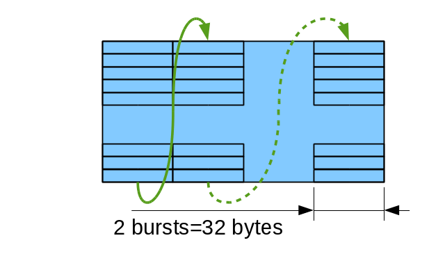
- Consolidate multiple accesses to the same page. In the simplest form (common for the camera designs) write consecutive memory locations (like fill memory with the scan-line data from the sensor). With 16-bit wide memory it is possible to transfer up to 2048 bytes at the full memory bandwidth with just one “activate” in the beginning and one “precharge” (or auto-precharge) in the end.
- Design the memory addressing in such a way, that translation of the linear address to physical bank, page number (“row address” in DRAM terminology) and in-page address (“column address”) makes it likely to simultaneously operate multiple banks.
While the first clue is easy to follow, the second one is not. Depending on the particular clock speed/timing parameters, you may need 3-5 banks to interleave to provide full data bandwidth utilization, something rather difficult to achieve for random data access without making special assumptions about the nature of the application data.
Camera deals mostly with the 2-d data arrays and majority of scenarios use either sequential (scan-line ordered) access or depend on 2-d locality of the pixels (compression, de-warping, correlation, filtering, and more). This mode can use tiled access and read/write small rectangular pixel areas as atomic operations. Contrary to the general processing memory, latency is not usually critical for the image memory, access patterns are predictable and can be pre-optimized in advance, not at the run time during memory access.
This allows to optimize a custom memory controller dedicated to image acquisition, processing and compression, and in our case support multiple image sensors operating in parallel. Particular application may include optical image-guided UAVs and other robotic devices.
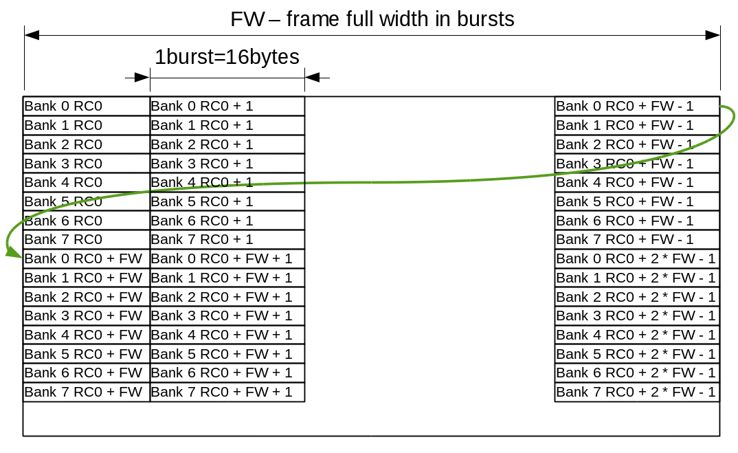
Mapping of the 2-d imaging objects to the DRAM memory addresses targets both sequential and tiled accesses. Each image scan line uses a single bank address (0..7) and increasing column addresses (2048 bytes or 128 bursts), then row addresses. Each group of 8 lines share the same row/column addresses and have individual banks for each row as shown on Fig.1.
Figure 1. Memory layout for 2-d image objects
Atomic memory accesses are currently limited to ¼ of the 4KB BRAM memory blocks available in Xilinx Zynq FPGA part, that makes 64 bursts or ½ of the memory page. Crossing page boundary during sequential access requires precharge and activation of the different memory pages in the same bank, so while the code can split accesses automatically it is beneficial to align the full frame width to the multiple of the 64 bursts (1024 8-bit or 512 of 16-bit pixels).
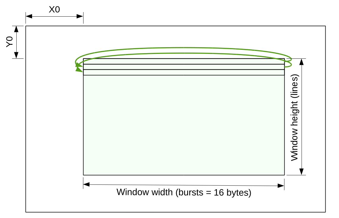
Scanline frame accessMemory controller provides application modules with a scanline windowed access to the image frames defined by the memory start address and the full (possibly padded) frame width, measured in 16-byte bursts. Access window is defined by conventional X0, Y0, width (in bursts) and height (in lines/pixels).
Figure 2 Access window in scanline mode
Scanline access module splits the requested window into a sequence of up to 64-burst data transfers, generates “page ready”, “frame ready” signals to application module, accepts “frame start”, “next page” signals. It also supports inter-channel synchronization by providing “next line number” output and “suspend” input. External module can compare last line number acquired from the sensor input channel and suspend compressor/image processing module, providing low-latency video.
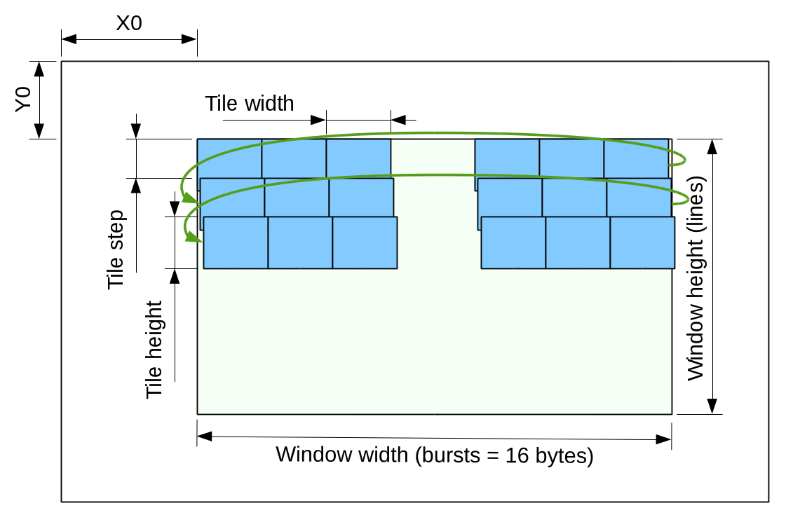
Tiled frame accessMany image processing and compression algorithms consume or generate 2-d blocks(tiles) of data. Some applications require overlapping tiles, including regular JPEG compression of color images. While compression algorithm itself uses non-overlapping 8×8 pixel blocks (16×16 macroblocks for 4:2:0 mode), extra pixels around the blocks are needed for Bayer-to-YCbCr conversion that is convenient to implement right in front of the compressor where the data is already available in 2d format, not in scanline order as it comes out of the sensor.
Figure 3 Access window in tiled mode
Tile overlap is needed both horizontally and vertically, but horizontal overlap is easy to implement in the application module just by using already buffered (in FPGA BlockRAM) data from the previous tile, while vertical overlap would need buffering the whole width of the sensor that would be not scalable for high resolution sensors and would require extra BlockRAM modules in the fabric. This is why the memory controller module provides only vertical tile overlap, accepting 3 byte-wide (width is limited by the total “area” of 64 bursts in a tile) parameters – tile width, tile height and tile step in addition to X0, Y0, window width and window height.
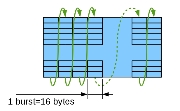
Tile internal structureMemory controller provides support for the 2 types of tiles. First type (Tile16) maps data to the sequence of bursts as vertical columns, each burst representing horizontal row of 16 (8-bpp mode) or 8 (16bpp mode) pixels.
Figure 4a: Tile16 – tile with 1 burst-wide columns
Figure 4b: Tile32 – tile with 2 burst-wide columns
Columns are traversed up to down, then left to write as shown on Fig. 4a. Due to memory timing restrictions this mode allows only some values for the tile height (0,6 and 7 modulo 8). Tile32 allows more variants for the tile height as there is more clock cycles between re-opening different page for the same bank, it can be (0,3,4,5,6,7 modulo 8). All tiles with the height of less than or equal to 8 are valid as it is possible to keep all banks open between columns of a tile, all heights are valid for the single-column tiles too. Single-column tile32 of maximal size (64 bursts) corresponds to a square area of 32×32 pixels in 8 bits per pixel mode.
NC393 HDL code and the memory controller implementationElphel camera code is built around the 16-channel DDR3 memory controller and at this stage the only modules that are not part of this controller are command and status distribution networks, system memory to external memory bridge over AXI_HP and temporary test modules to test controller functionality.
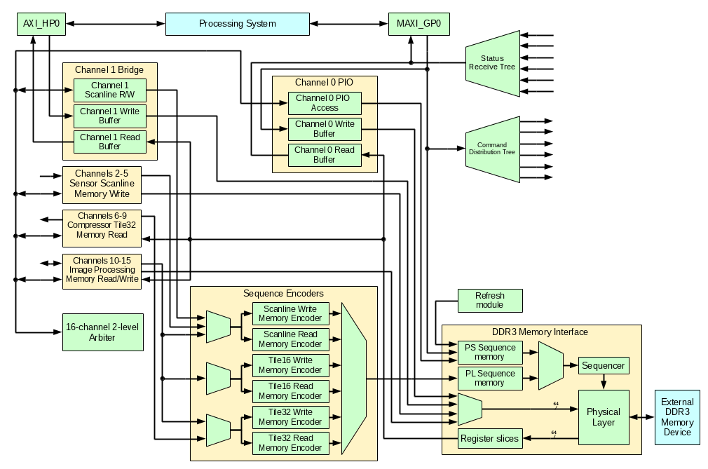
Figure 5. Memory controller block diagram
Command and status networksCommand distribution tree is designed to write data to various memory-mapped registers distributed over the whole design. All these registers are write-only (readback is optionally provided by a separate Block RAM-based module), so data paths can accommodate any number of register slices if needed to meet timing. This bus is a light-weight to minimize required routing resources of the FPGA, it requires only 9 data signals (9 address/data and a strobe) and can deliver 0 to 32 bits of data (configured by parameters at the destination module) sent over 1 to 6 clock cycles. Command distribution tree accepts commands from the software over the MAXI_GP0 or from a PL sequencer driven by the frame synchronization signals from the sensors – it will be ported from the current NC353 camera HDL code.
Status receive tree supplements the command tree and provides processing system with a feedback data from the distributed over the FPGA fabric modules. It includes a 256×32 register file available for PS read access with zero latency and a unidirectional tree of light-weight (10 signals) network that also includes multiplexers and status transmitters. Multiplexers route the messages (up to 6 clock cycles long depending on a payload) to the terminating register file. Status transmitters (controlled through the command distribution network) provide means to synchronize responses to the PS requests using 6-bit IDs, they send up to 26-bit status information either in response to a command or automatically when the input data changes.
Memory interface is forked from an earlier eddr3 project (there are some important bug fixes). In addition to the physical layer components it includes sequencer that generates address and control signals for memory device access following the program data prepared in advance. This sequence programs come from one of the two sources – PS Sequence Memory written under the software control and PL Sequence Memory filled in by one one of the Sequence encoders just before (during previous memory transaction) the execution. Both memories are made of 4KB Block RAM modules. PS sequences are used for memory refresh access instructions, memory initialization and calibration, any other pre-programmed memory operations that need to be executed following specific timing.
Memory interface is configurable with Verilog `define macros and can interface up to 16 concurrent channels, each being read-only, write-only or bidirectional. Each channel is supposed to have a 4KB block RAM buffer (or two of them for bidirectional channels) configured in SDP (simple dual port) mode with 64-bit wide input (for memory read) or 64-bit output (for memory write). Memory interface also provides channels with clock and control signals for the memory side of the buffers, other side of these dual-port buffers is under channel logic control, it may be clocked by a different source. Two layers of registers may be inserted in both input (16:1) multiplexer path and output distribution of the 64-bit wide data buses that may need routing to different parts of the device.
Channel buffers are based on 4KB block RAM modules, each split into 4 of 1KB pages, making them suitable for up to 64 of 16-byte bursts transfers. Of the four pages one (in some overlapping tiles applications – two) is in use by the channel logic (being consumed or generated), another is used by the transfer to/from the DRAM memory, and the remaining ones provide needed buffering when memory is in use by the other channels.
16-channel arbiter accepts two levels of urgency (“want” and “need” signals) from the channel controllers. In most cases memory read channels generate “need” if there is at least one empty buffer page and the channel will need it later (not the last pages in a frame), “need” is generated when the channel is consuming the last available page. Similarly for the memory write channels – “want” is generated when there is at least one completed page, “need” – when there is no empty pages left. Channels that can wait for the data can skip raising the “need” signal leaving more resources to other channels that are tied to constant data rate data (such as inputs from the sensors).
In addition to the two levels of urgency (channels with ”need” requests are served before “want” ones compete) arbiter provides channel priorities. Each channel has associated counter that increments at each event (new request or request grant), taking care of the simultaneous requests by static priority by channel number. The channel having highest counter value wins, receives “grant” signal and that channel counter is reset to the specified channel priority value, so priority 0 makes that channel to wait maximal time.
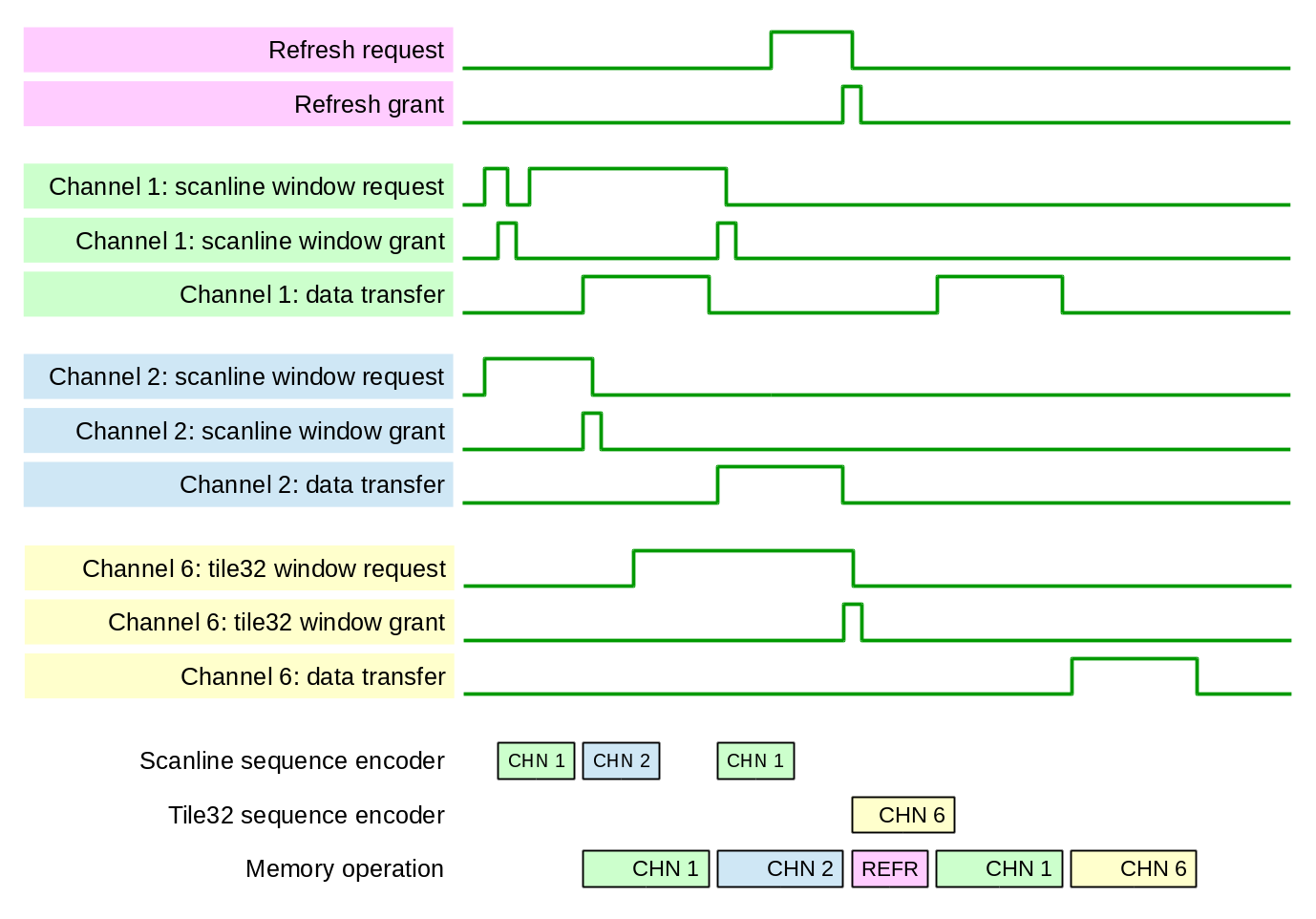
Figure 6. Memory access arbitration and timing
Sequence generation takes less time than the actual memory access, and channel arbitration happens when the previous sequence data is sent for execution. Fig. 6 shows that channel 2 sequence is started to be transferred to the PL Sequence Memory as soon as the memory interface starts to execute sequence for channel 1.
There is an additional arbitration just before starting to execute a sequence – if refresh module (it does not need to transfer sequence data as it is already in the PS Sequence Memory) generates “want” or “need” request, it competes against the already granted channel that has the sequence ready to be executed – Fig. 6 shows how REFR sequence passes the CHN1 that is ready to be executed. The sequence FIFO in PL Sequence Memory allows only one sequence to be buffered. This limit is imposed to reduce waiting for service of the urgent (“need”) requests while not using a more complicated mechanism that would allow such requests to pass other channel non-urgent (“want”) requests in the sequence memory FIFO. It is still a possibility for the future improvements to allow efficient execution of significantly different size memory transfers.
Sequence encoders are shared between the channels – the channel that wins the arbitration is granted to generate a memory access sequence. Currently there are 6 of such modules that generated scanline read, tile16 and tile32 (see Fig. 4a-b) and similar for memory writes. These modules accept address and size parameters from the window access controllers and use HDL-encoded templates to generate control sequence for the next memory access operation.
Channel window access controllersWindow access controllers implement access to selected rectangular areas inside the image frame. There are two types currently available – scanline access (Fig. 2) and tiled access (Fig.3). Distinction between read and write modes, and between tile16 and tile32 modes are passed as run-time parameters. They are used later to select the specific sequence encoder each time the request is granted by the arbiter. These modules require individual instances for each channel that uses them as they have to keep track of the related channel buffer, tile location and other module state variables.
Additional controllers will be developed for other types of accesses when needed by the image processing algorithms that may need other types of memory accesses. Example application may be a distortion correction procedure where either input or output use tiles that are not defined by a regular grid).
Channel 0 is designed for programmable access to the memory. It uses PS Sequence Memory written through MAXI_GP0 under the software control. It has both read and write buffers for operations that involve data transfer, it is used for memory initialization and calibration/training, it can also be used to test other access sequences without re-generation of the bitstream.
Channel 1 implements a fast bi-directional bridge between the system memory and the dedicated image memory. On the system side it uses AXI_HP0 port in 64-bit mode, on the image memory side it implements a scanline window access It is possible to either fill the selected window in the image memory with the consecutive data from the system memory, or read image memory window to a linear array in the system memory.
Channels 2-5 will be used to record data from the four sensor ports, currently one channel is connected to 2 buffers connected to the SAXI_GP0 interface for testing scanline windowed memory access.
Channels 6-9 will be used in tile32 mode to read 2d data for image compression. Temporary implementation uses 2 channels connected to SAXI_GP0 read/write for testing purposes.
Remaining six channels may be used for application-specific image processing.
The list of the tools used for this project is the same as listed for the earlier eddr3 project. The only difference is that now it is Eclipse Luna instead of Kepler, and some bugs in VDT plugin are fixed – bugs that revealed themselves while this plugin was being used with gradually growing code base.
The x393 project code itself is available under GNU GPLv3 Free Software license, does not depend on any undocumented or encrypted “IP” modules and can be simulated with the Free Software tools. Project configuration files allow importing it to Eclipse IDE when VDT plugin is installed.
FPGA to DDR3 memory interface: step-by-step timing calibration and set up
Working with the DDR3 Memory interface I was not able to avoid the temptation to investigate more the very useful feature of the modern FPGA devices – individually programmed input/output delay elements on all (or at least many) of its pins. This is needed to both prepare to increase the memory clock frequency and to be able to individually adjust the timing on other pads, such as the sensor ports, especially when switching from the parallel to high speed serial interface of the modern image sensors.
Xilinx Zynq device we are using has both input and output delays on all low-voltage pins used for the memory interface in the camera, but only input ones on the higher voltage range I/O banks. Luckily enough image sensors connected to these banks need just that – data rate to the sensors is much lower than the rate of the data they generate and send to the FPGA.
Adjustment of the optimal pin delays for the memory interface can be done in several ways, and many applications require that it should be either all implemented in hardware or use very limited CPU resources – that is the case when the memory to be set up is the main system memory and so CPU can not use it. On the other hand when the memory is connected to the FPGA part of the system that is already running with full software capabilities it is possible to use more elaborate algorithms.
I call it for myself “the Apple ][ principle” - do not use extra hardware for what can be done in software. In the case of the delay calibration for the memory interface it should be possible to use a reasonable model of the delay elements, perform measurements and calculate the parameters of such model, and finally calculate the optimal settings for each programmable component. Performing full measurements and performing parameter fitting can be a computationally intensive procedure (current Python implementation runs 10 minutes) but calculating the optimal settings from the parameters is very simple and fast. It is also reasonable to expect that individual parameters have simple dependence on the temperature so it will be easy to adjust parameters to the varying system temperature. Another benefit of such approach that it can use delay elements with even non-monotonic performance (that is sometimes in case when using FINEDELAY elements) and finally – the internal parameters of the delay elements do not depend on the clock frequency, so parameters can be measured at lower clock frequency and then settings can be re-calculated for the higher one. Adjusting timing parameters at the target frequency can be more difficult as there can be much smaller windows of the combination of the parameters that allow memory device to operate, it may be not possible to probe marginal values of some delays (to calculate the optimal center value) as it may violate other timing parameters.
The procedure described below can be used to measure the delay parameters of the memory interface and find the optimal combinations of the settings requiring no manual adjustments of the initial values. The software is written in Python and is a part of the Elphel GitHub repository x393 as x393/py393 PyDev project.
The Python code includes a module that can parse Verilog header files with parameter definitions so all the changes in the HDL code are automatically applied to the Python program, running the program on the target hardware generates updated values of the delay settings as a Verilog file, so these measured values can be used in simulation. This program is of course designed to run on the target platform, but most of the processing can be tested on a host computer - the project repository contains a set of measured data as a Python pickle file that can be loaded in the program with a command "load_mcntrl dbg/x393_mcntrl.pickle". Program can run automatically using the command file provided through the arguments, it also supports interactive mode. Most of the functions defined in the program modules are exposed to the program CLI, so it is possible to launch them, get basic usage help. Same is true for the Verilog parameters and macro defines - they are available for searching and it is possible to view their values.
Delay elements in the memory interface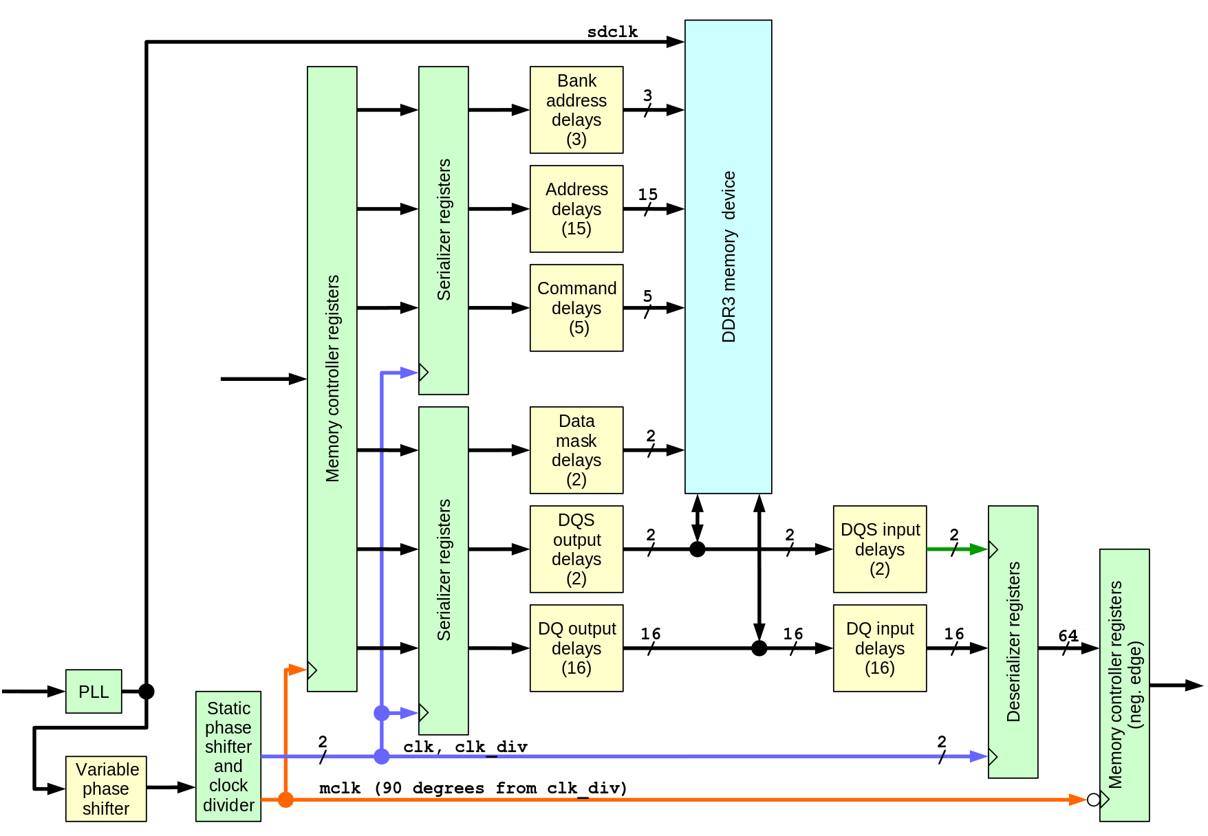
Fig.1 Memory interface diagram showing signal paths and delays
There are total 61 programmable delays and a programmable phase shifter as a part of the clock management circuitry. Of these delays 57 are currently controlled – data mask signals are not used in this application (when needed they can be adjusted by the similar procedure as DQ output delays), ODT signal has more relaxed timing and the CKE (clock enable) is not combined with the other signals. There are 3 clock signals generated by the same clock management module with statically programmed delays: clk (same frequency as the memory clock), clk_div (half memory frequency) and mclk – also half frequency, but with 90 degree phase shift with respect to clk_div, it is driving the memory controller logic. Full list of the clock signals and their description is provided in the project.
Variable phase shifter (with the current 400 Mhz memory clock it has 112 steps per full clock period) is essentially providing variable phase clock driving the memory device, but to avoid dependence on the memory internal PLL circuitry, memory is driven by the non-adjusted clock, and programmed phase shift is applied to all other clock signals instead.
Address/control signals and data to be written to the memory device originate in the registers and Block RAM of the controller running at mclk global clock, then they go through serializers (OSERDESE2 for synthesis, OSERDESE1 for simulation to avoid undisclosed code modules). Serializers use two clocks and in this design the slower clk_div is ¾ of the mclk period later than mclk itself to guarantee positive setup time when crossing the clock boundary. Serializers for data, data mask and DQS strobes operate in DDR mode, while the ones for address and command signals use single data rate mode. Each of this signals pass through individual 32-tap delay with nominal 78 ps/step, followed by a a 5-tap fine delay element (ODELAYE2_FINEDELAY) and then go to the external memory device.
On the way back the data read from the memory and the read strobes (one per each data byte) pass through IDELAYE2_FINEDELAY elements and then strobes pass through BUFIO clock buffers that drive input clock ports of the deserializers ( ISERDESE2 for synthesis, ISERDESE1 for simulation), while the same (as used for the output serializers) clk and clk_div drive the system-synchronous ports. When crossing clock boundary to the mclk registers that receive data from the deserializers use the falling edge of mclk and there is again ¾ of mclk period to guarantee positive setup time.
The delay measurement procedure involves varying the delay that has uniform phase shift step (1/112 memory clock period) and adjustment of the variable “analog” pin delays that have some uncertainty: constant shift, scale (delay per step) and non-linearity. The measurement steps that require writing data to the memory and reading it back, and so depending on the periodic memory refresh, the automatic refresh is temporarily turned off when the clock phase and command delays are modified.
Measuring delays in the signal paths and setting memory interface timing Step 1 : Finding valid command/address delays for each clock phase settingThe first thing to do to be able to operate the memory is to find the address/command line delay that is safe to use with each clock phase and/or find what values of the phase shift are valid. The address and command signals use single data rate (sampled at the leading edge of the clock by the memory device) so it is easier to satisfy the setup/hold requirements than for the data. DDR3 devices provide a special “write levelling” mode of operation that requires only clock, address/command lines and DQS output strobes providing result on the data bus. At this stage timing of the read data is not critical as the data data stay the same for the same DQS timing, and it is either 0×00 or 0×01 in each of the data bytes.
It is possible to try reading data in this mode (reading multiple data words and discarding groups of first and last one no remove dependence of read data timing) and if the result is neither 0×00 nor 0×01 then reset the memory, change the command delay (or phase) by say ¼ of the clock period, and start over again. If the result matches the write levelling pattern it is possible to find the marginal value value of the address delay by varying delay of address bit 7 when writing the Mode Register 1 (MR1) – this bit sets the write levelling mode, if it was 0 then the data bus will remain in high impedance state.
Fig.2 Finding the command/address lines delay for each clock phase
Memory controller drives address lines in “lazy” mode leaving them unchanged when they are not needed (during inactive NOP commands) so it is easier to check if A[7] low → high transition happens too late. Additionally the tested write levelling command have to be preceded by some other command with A[7] at low level.
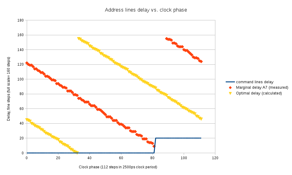
Figure 2 shows the process of scanning over phases and finding the longest delay on A[7] line that still turns on the write levelling mode (shown with red diamonds). Command line delays are kept at zero until at phase 82 the delay on A[7] line becomes smaller than a preset limit (command lines are almost too late themselves), at this phase the command line delay is increased so the command is recognized in the next clock cycle and so the marginal value of A[7] is also increased by the full clock period. With the current settings the full delay range is almost exactly equal to the clock period, this will not be the case at higher memory clock rates (delays will cover more than a period) or increasing the delay calibration clock rate from 200 MHz to 300 MHz (delays will cover les than a period). On the Figure 2 there is a small gap (to phase=86) when the marginal delay for A[7] can not be measured as it would exceed the maximal delay value available in OSERDESE2 element.
Yellow triangles show the optimal values for the A[7] delay calculated by applying linear interpolation to the marginal values and shifting the result horizontally by ½ of the clock period (56 phase steps).
At this preliminary stage optimal command/address delays are assumed to be the same as for the A[7] – they are connected to the same I/O bank. Later it will be possible to optimize each signal delay individually, when switching to the higher frequency the relative differences between lines can be assumed the be the same and can be applied accordingly.
During the next stages of the delay measurement the command and address lines delay values are all set whenever the clock phase is changed.
Step 2: Measuring individual delays for command (RAS,CAS,WE) lines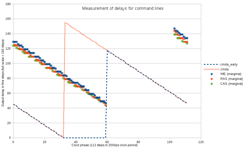
Fig.3 Command lines delays measurement
When the approximate value for the optimal delay for the address/command lines is known it is possible to individually calibrate delay for the command lines. The mode register set command involves high (inactive) to low (active) state on all 3 of them, so it is possible to probe turning on the write levelling mode when 2 of the the 3 command lines (and all the bank and address lines) are set with the optimal values, while the delay on the remaining command line is varied. Sometimes this procedure leads to the memory entering undefined/non-operational state (write levelling pattern is not detected even after restoring known-good delay values), when such condition is detected, the program resets and re-initializes the memory device.
To increase the range of the usable phases the other command/address lines are kept at delay=0 while there still is a safe margin of the setup time with respect to memory clock (from phase = 32 to 60 on Fig. 3)
Step 3: Write levelling – finding the optimal DQS output delays for clock phase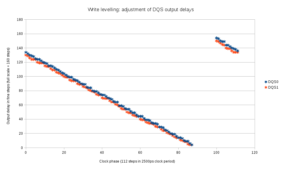
Fig.4 DQS output delay measurement with write levelling mode
This special mode of DDR3 devices operation is intended to adjust the DQS signal generated by the controller to the clock as seen by the memory device, it measures clock value at the leading edge of the DQS signals and replies with either 0×00 (clock was low) or 0×01 (clock was high) on each data byte of DQ signals.
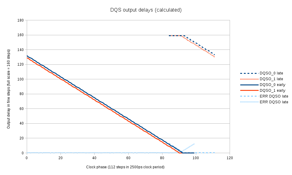
Fig.5 Calculated optimal DQS output delays for each clock phase
The clock phase is scanned over the full period and for each phase the marginal (switching from 0×00 to 0×01) DQS output delay is measured for each of the byte lanes. This procedure directly results in the optimal values of the DQS output delay values, there is no need to shift them by a half-period. Fig. 5 shows the calculated by linear interpolation values of the DQS output delays for each phase. To increase the range of DQ vs. DQS delay measurements, the DQS output signals are allowed to slightly deviate from the optimal – Fig. 5 shows “early” and “late” branches and the amount of deviation.
The similar calculation is performed later once more time when additional data from co-measurement of DQ output delays and DQS output delays becomes available. At that stage it is possible to account for non-uniform fine delay steps of DQS output lines.
Step 4: Fixed pattern measurementsDDR3 memory devices have another special operational mode intended for timing set up that does not depend on actual data being written to the memory or read back. This is reading a predefined pattern from the device, currently only one pattern is defined – it is just alternating 0-1-0-1… on each of the data lines simultaneously. In this step the 11 of the 8-word bursts are read from the memory, then only the middle 8 bursts are processed, so there is no dependence on the (yet) wrong timing settings that result in the wrong synchronization of the data bursts. That provides 64 data words, half being in even (starting from 0) positions that are supposed to be zeros, and half in odd ones (should read all 1-s), and then total number of ones is calculated for each data bit for odd and even slots – 16 pairs of numbers in the range of zero to 32. These results depend on the difference between delays in the data and data strobe signal paths and allow detection of 4 different events in each data line: alignment of the leading edge on the DQ line to the leading edge of the DQS signal (as seen at the de-serializer inputs), trailing edge of the DQ to leading one of DQS and the same leading and trailing DQ to the trailing DQS. They are measured as transitions from 0 to 1 and from 1 to zero separately for even and odd data samples.
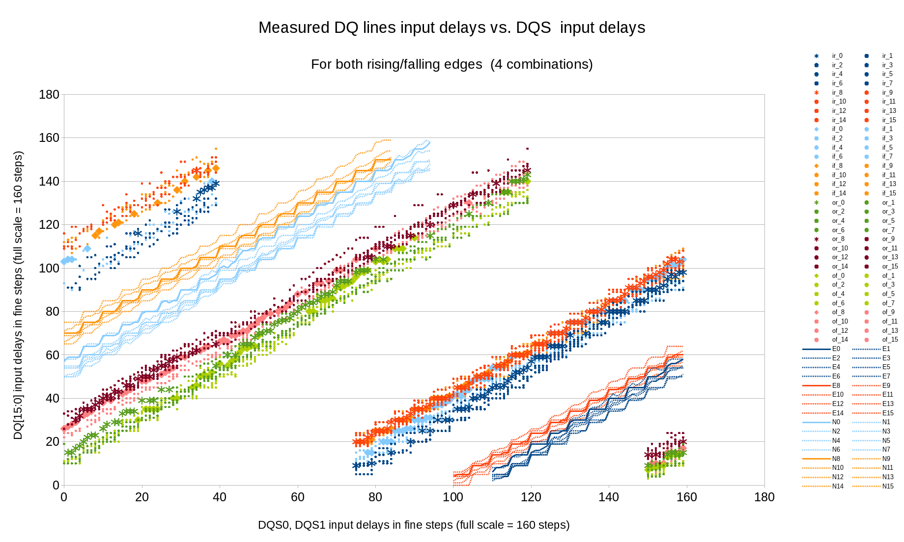
Fig.6 Measured (marginal) and calculated (optimal) DQ input delays vs. DQS input delays
Most results have 0 or 32 values (all data words are read 0 or 1), but some provide intermediate “analog” results when corresponding words are read differently, depending on some uncontrolled factors. Later processing assumes that the difference from the middle value (16) is proportional to the difference between the measured (by the settings) delay value and the actual one. Additionally if the number of such analog samples is sufficient, it is possible to process only them and discard “binary” (all 0-s/all 1-s transitions).
This measurement can be made with any clock phase setting. Even as normally there is a certain relation between the phase and DQS delay (measured in the next step), wrong setting shifts read data by the full clock period or 2 bits for each DQ line, with 0-1-0-1 pattern there is no difference caused by such shift and we are discarding first and last data bursts where such shift could be noticed.
Figure 6 shows measured 4 variants for each data bit, ‘ir_*” for in-phase (DQ to DQS), DQ rising, “if” in-phase DQ falling, ‘or’ – opposite phase rising and ‘of’ – opposite phase falling. Only “analog” samples are kept. “E*” and “N*” show the calculated optimal DQ* delay for each DQS delay value. Calculation is performed with Levenberg-Marquardt algorithm with the delay model describe late in this article, the same program method is used both for input and output delays. The visible waves on the result curves are caused by the non-uniformity of the combined 32-tap main delays with the additional 5-tap fine delay elements, different amplitude of these waves is caused by the phase shift between the DQ and DQS lines (“phase” here is the fine delay (0..5) value – the full 0..159 delay modulo 5).
Step 5: Measuring DQS input delay vs. clock phaseDeserializers use both memory-synchronous clock (derived from DQS) and system-synchronous clk and clk_div, so there is a certain optimal phase shift between the two, allowing maximal deviation of the memory-synchronous input clock.
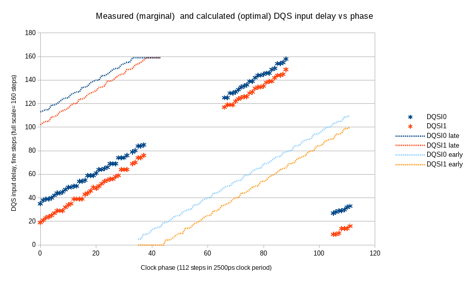
Fig.7 Measured (marginal) and calculated (optimal) DQS input delays vs. clock phase
Data is crossing clock domains boundary at a single clock rate (2 bits at a time for each data line), so using fixed pattern of alternating 0-1-0-1… can not be used – regardless of the phase shift it will be the same “01” pair. For this reason we use actual read data command, not a special read pattern mode. Random data that is present in the memory array after power up can be used, but the program is writing a 0-0-1-1-0-0- 11… pattern for each data bit. This pattern will provide different di-bit value in each DQ line, even if the write DQ to DQS timing is not yet determined, so the actual data can be any of X-0-X-1-X- 0… where X can quasi-randomly be any of 0 or 1. The pattern is recorded once, then the data is read with different DQS input delays (DQ input delays are set according to step 4 results), comparing only the middle portion with the beginning/end discarded as before. The marginal DQS delay is detected as the value when the read data changes from the original value.
Figure 7 shows results of such measurements as well as the calculated optimal input delays for DQS lines. This calculation uses both Step 5 (DQS vs. phase) and Step 4 (DQ vs. DQS) measuremts and accounts for the fine delay non-uniformity.
Step 6: DQ to DQS output delays measurements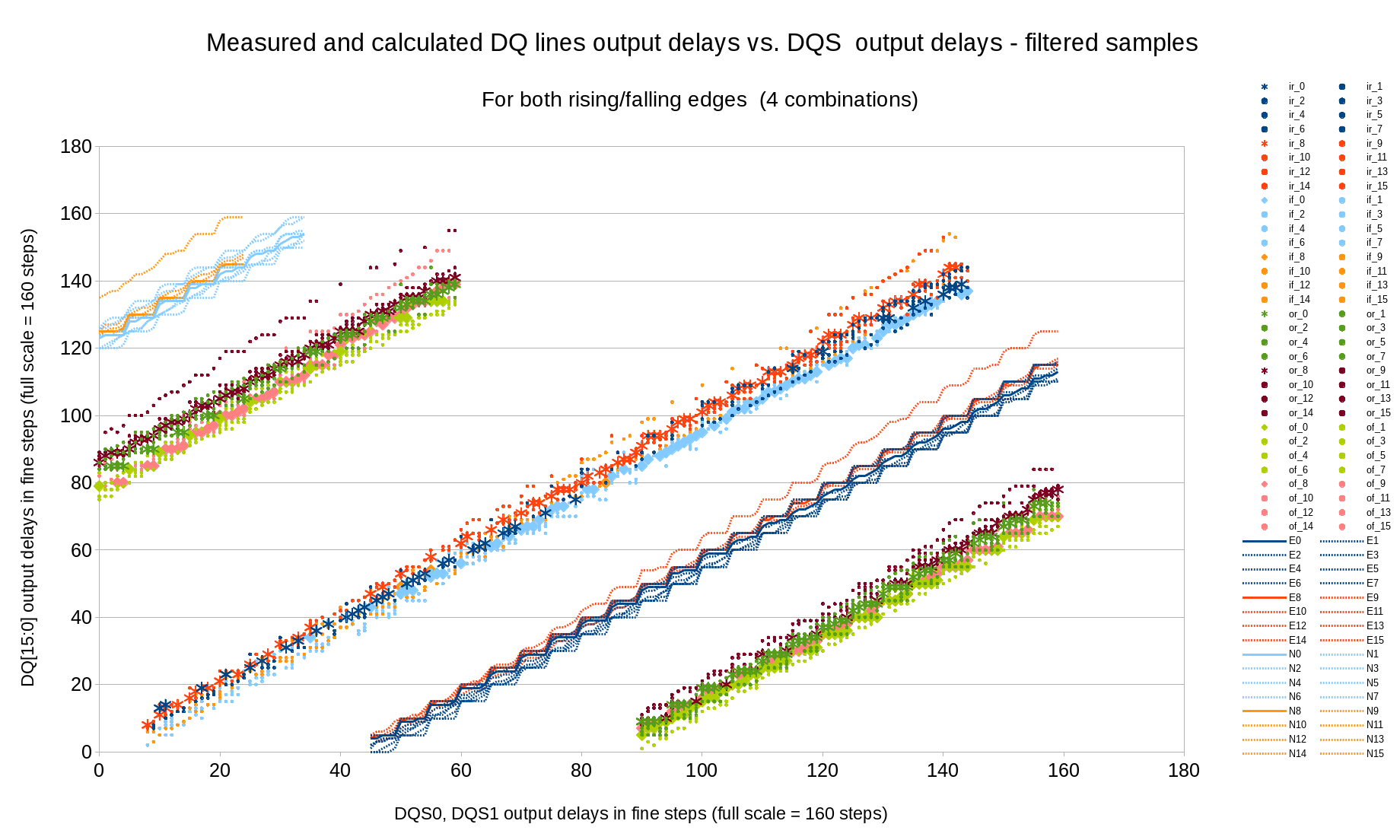
Fig.8 Measured (marginal) and calculated (optimal) DQ input delays vs. DQS output delays
This measurement is performed similarly to step 4 when DQ to DQS input delays relation was probed with a fixed pattern readout mode. Now we already have known settings for the memory read operation and can rely on it to adjust write mode (output) delays. Alternating 0-1-0-1 sequence in every line similar to the pattern mode is recorded with various DQS output delay values, for each DQS delay appropriate phase and address/command delay values are used. Input delays (for DQS and DQ) are set for each phase using data from the previous steps and the data written with different DQ output delay is read back, then processed in the same way as in Step 4.
Figure 8 presents the relation between DQ and DQS output delays, and the result of combining Step 6 measurements with Step 3 (write levelling) – optimal DQ and DQS output delay values for different clock phase can be seen on Figure 9 that shows all the delays. Allowing some deviation from the DQS to clock alignment (this requirement is more relaxed than DQ-to-DQS delays) results into 2 alternative solutions for the same phase shift near phase=95, use of the higher memory clock rates will result in more of such multi-solution areas even without deviation from the optimal values.
Step 7: Measuring individual output delays for all address and bank linesHaving almost calibrated read and write memory operations it is now possible to set up output delays for each of the remaining address and bank lines (so far only A[7] was measured, other lines were just assumed to be the same). This measurement is done with writing some “good” pattern to a specific bank/row/column page (column address uses the low bits of the row address), and a “bad” data to all pages different by 1 of the address or bank bits. For this test the refresh sequence (it is loaded by the software, it is not hard-wired in the HDL code) was modified to provide specified data on the bank/address lines that is “don’t care” for this operation. These values are set to be inverted values to the “good” address, and the refresh command was manually requested before the read operation, making sure that the command will cause all the address/bank bits to be inverted.
All the phase values are scanned, for each phase the command and address delays are set to the optimal values as defined so far, and only one line at a time delay was modified to find the marginal value that causes the readout of the wrong data block.
This measurement is performed twice – fist with “good” address of all zeros, then – with all ones and results averaged for low → high and high → low address line transitions.
Step 8: Selecting valid parameter combinations for readout and write modes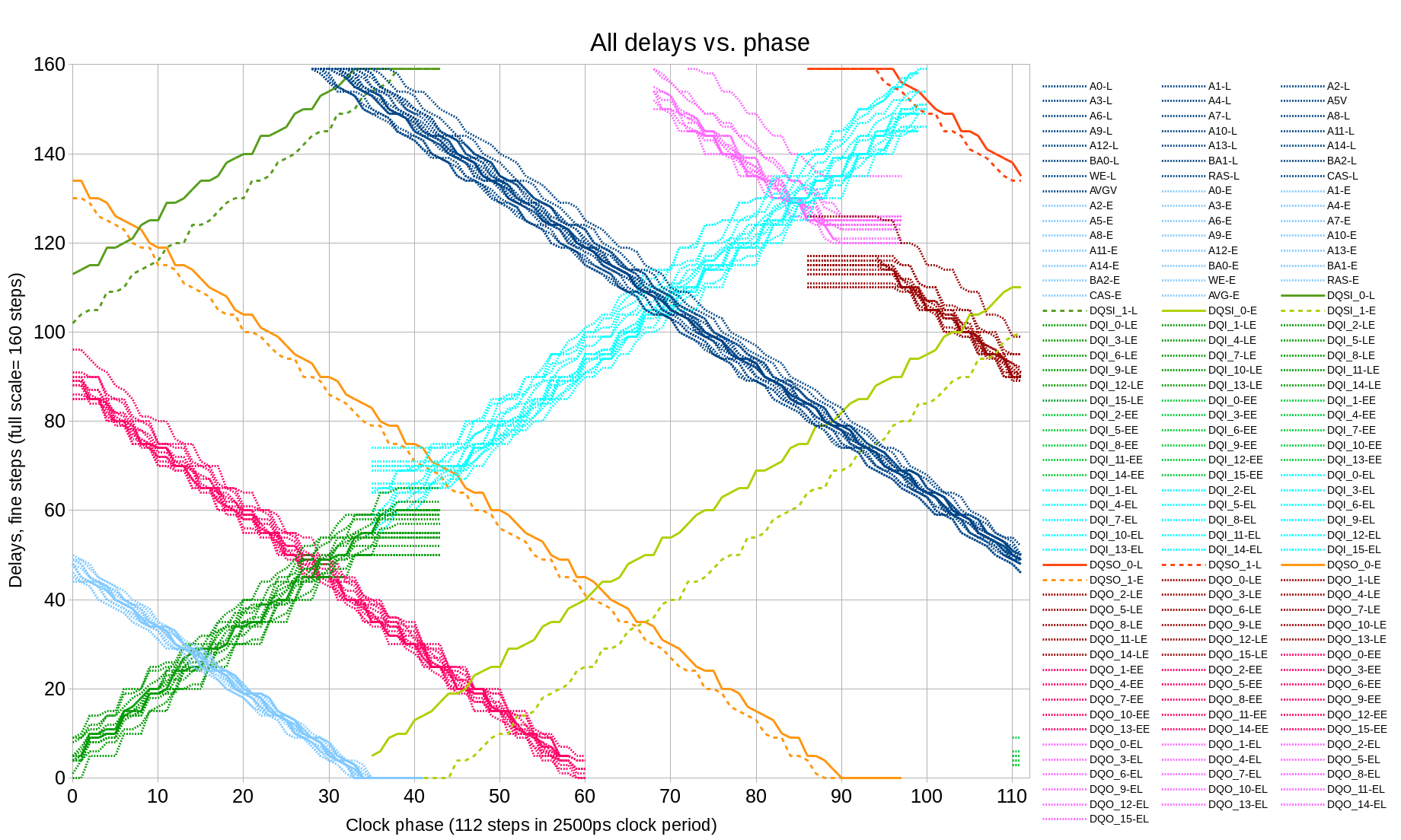
Fig.9 All delays vs. clock phase
Figure 9 combines all the data acquired so far as a function of the clock phase shift. Most of the delays do not change when the new bitstream is generated after the modification of the HDL code – the involved delays are defined by the fixed I/O circuitry and PCB/package routing. Only two of the signals involve FPGA fabric routes – DQS input signals that include BUFIO clock buffers, these buffers can be selected differently and routed differently by the tools. These signals also show the largest difference one the graph (two pairs of the green lines – solid and dashed).
There are additional requirements that are not shown on the Figure 9. DQ signals from the memory should arrive to the deserializer ¼ clock period earlier than the leading edge of the first DQS pulse, not 1 ¼ or not ¾ later – the measurements so far where made to the nearest clock period. Memory device generates exactly the required number of DQS transitions, so if the data arrives 1 clock too early, then the first two words will be lost, if it arrives 1 clock too late – the last two words will be lost.
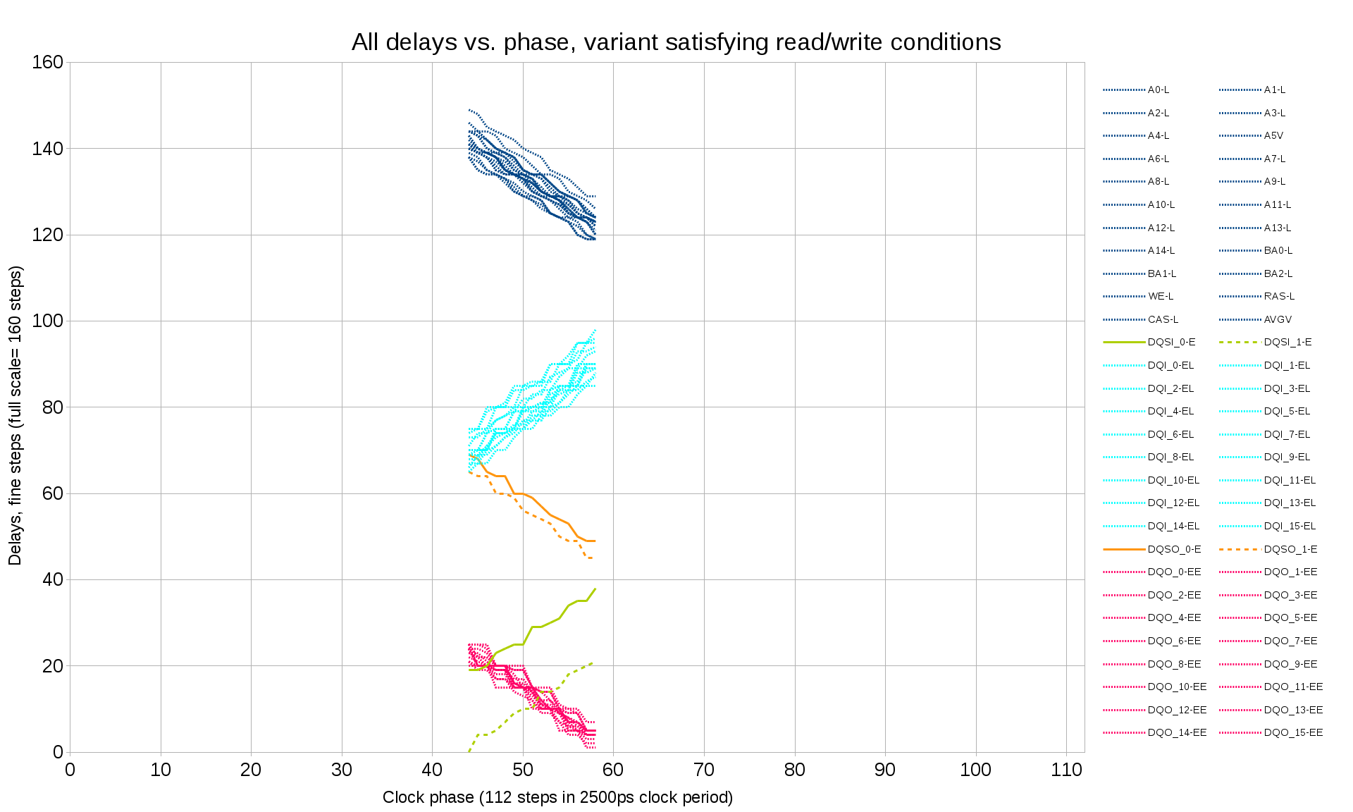
Fig.10 All delays vs. clock phase, filtered to satisfy period-correct write/read conditions
For this final step the alternative variants of the setting that differ by the full clock periods are selected and tested. First the block with incremented (each word is the previous one plus 1) data is recorded and then the smaller block completely inside the recorded one and not using the first/last bursts is read back. The write mode is not yet set up, so the first/last recorded burst can not be trusted, but the middle ones should be recorded incrementally, so any differences from this pattern have to be caused by the incorrect readout settings.
After removing invalid parameter combinations defining the readout mode we can trust that the full block readout has all the words valid. Then we can do the same for the write mode and check which of the variants (if any) provide correct memory write operation. In the test case (one particular hardware sample and one clock frequency there was exactly one variant (as shown on the Figure 10) and the final settings can use the center of the range. With higher clock frequency several solutions may be possible – then other factors can be considered, such as trying to minimize the delays of the most timing-critical signals (DQ, DQS) to reduce dependence on the possible delay vs. temperature variations (not measured yet).
Model and parameters of the input/output delay elementsProcessing of the measurement results in steps 4 and 6 involved using a delay model defined by a set of parameters and then finding the values of these parameters to best fit the measurement results.
Each data byte lane is independent from the other, so for each of the 4 groups (two for output and two for input) there are nine signals – one DQS and 8 DQ signals. Each delay consists of a 32-tap delay line with the datasheet delay of 78 ps per tap and a 5-tap delay with nominal 10 ps step. Our model represents each 32-tap delay as linear with tDQ[7:0] delays corresponding to a tap 0 and tSDQ[7:0], tSDQS – individual scale (measured in picoseconds per step). Fine delay steps turned out to be very non-uniform (in some cases even non-monotonic) so each of the 4 delay values (for 5-tap delay) is assigned an individual parameter – 4 for DQS (tFSDQS) and 32 for DQ (tFSDQ).
Procedure of measuring all 4 combinations of leading/trailing edges of the strobe and data makes it possible to calculate duty cycle for each of the 9 signals – tDQSHL (difference between time high and time low for the DQS signal) and eight tDQHL[7:0] for the similar differences for each of the data lines. Additional parameter was used to model the uncertainty of the measurement results (number of ones or zeros of the 32 samples) as a function of the delay difference from the center (corresponding to 50% of the zeros and ones). This parameter (anaScale in the program code) is measured in picoseconds and means how much the delay should be changed to switch form all 0 to all 1 (using simple piecewise linear approximation).
Parameter fitting is implemented using Levenberg-Marquardt algorithm, initial scale values use dataseeet data, initial delays are estimated using histograms of the acquired data (to separate data acquired with different integer number of clock cycles shift), other parameters are initialized to zeros. Below is a sample of the program output – algorithm converges rather quickly, getting to the remaining root mean square error (difference between the measured and modeled data) of about 10ps:
Before LMA (DQ lane 0): average(fx)= 40.929028ps, rms(fx)=68.575944ps
0: LMA_step SUCCESS average(fx)= -0.336785ps, rms(fx)=19.860737ps
1: LMA_step SUCCESS average(fx)= -0.588623ps, rms(fx)=11.372493ps
2: LMA_step SUCCESS average(fx)= -0.188890ps, rms(fx)=10.078727ps
3: LMA_step SUCCESS average(fx)= -0.050376ps, rms(fx)=9.963139ps
4: LMA_step SUCCESS average(fx)= -0.013543ps, rms(fx)=9.953569ps
5: LMA_step SUCCESS average(fx)= -0.003575ps, rms(fx)=9.952006ps
6: LMA_step SUCCESS average(fx)= -0.000679ps, rms(fx)=9.951826ps
Tables 1 and 2 summarize parameters of delay models for all input and data/strobe output signals. Of course these parameters do not describe the pure delay elements of the FPGA device, but a combination of these elements, I/O ports and PCB traces, delays in the DDR3 memory device. The BUFIO clock buffers and routing delays also contribute to the delays of the DQS input paths.
Table 1. Input delays model parameters
parameter
number of values
average
min
max
max-min
units
tDQSHL
2
4.67
-35.56
44.9
80.46
ps
tDQHL
16
-74.12
-128.03
-4.96
123.07
ps
tDQ
16
159.87
113.93
213.44
99.51
ps
tSDQS
2
77.98
75.36
80.59
5.23
ps/step
tSDQ
16
75.18
73
77
4
ps/step
tFSDQS
8
5.78
-1.01
9.88
10.89
ps/step
tFSDQ
64
6.73
-1.68
14.25
15.93
ps/step
anaScale
2
17.6
17.15
18.05
0.9
ps
I noticed the existence of these 5-tap delay elements in the utilization report of Xilinx Vivado tools – they do not seem to be documented in the Libraries Guide. I assume that the manufacturer was not very happy with their performance (the average measured value of the delay per tap turned out to be less than 7 ps so even the last tap output does not provide delay of the half of the 32-tap step, and non-uniformity of the delays makes it difficult to use in the simple hardware-based delay adjustment modules. But I like this option – it almost gives one extra bit of delay and as we are using software for delay calibration it is not a problem to have even a non-monotonic delay stage. So I would like to see this feature improved – added more taps to completely cover the full step of the coarse delay stage in the future devices, and have this nice feature documented, not hidden from the users.
Use of the internal voltage reference and the duty cycle correctionInternal reference voltage option was used in the tested circuitry because of the limited number of pins to implement a single-bank 16-bit wide memory interface, and the Xilinx datasheet limits memory clock to just 400 MHz for such configuration. Measurements show that there is a bias of -74.12ps on the duty cycle that may be caused by variation of the internal reference voltage, but the spread of the delays (123 ps) is still larger. Of course it is difficult to judge without having statistics on multiple units, but I suppose that the handicap of using internal reference is not that significant. And even 123ps is not that big as tDQHL was measured as a difference of duration high minus duration low, so if one transition edge is fixed, the other will have an error of just half of this value – less than a coarse (32-tap) delay when calibrated at 200 MHz (fine delay is possible to calibrate with 300MHz).
It would be nice to have at least a couple of bits in the delay primitives dedicated to the duty cycle correction of the delay elements that can be implemented as selective AND or OR the delay tap output with the previous one.
Kernel development for OpenEmbedded with Eclipse
Eclipse with C Development Tool (CDT) is a very powerful and feature-rich IDE for developing embedded Linux applications, such as Elphel393 camera. CDT includes CODAN — static code analysis tool which helps user to track possible problems in his code without compiling it, and Code Indexer, giving an auto-complete and code navigating (F3) features. They work independently from compiler, thus parsing the code in the same manner as compiler does is essential for producing meaningful results. As project grows, the interconnections between its parts tend to become more and more complicated, and maintaining the congruency of code processing for compiler and CODAN/Code Indexer becomes a non-trivial task. In the Internet, the most frequent recommendation for users who wish to develop Linux kernel with Eclipse is to disable CODAN feature since messy false error markers make it practically unusable. The situation becomes even worse for developers using external build tools (such as OpenEmbedded’s BitBake) as CODAN relies on output of a CDT-integrated build system to find correct way of code parsing. Anyway, embedded Linux applications usually involve kernel development, so we’ll try to find a practical approach to get the power of CODAN and Code Indexer into our hands.
Preparing the source code
I assume Poky image build environment is already set up. More info can be found here.
Main source of analysis errors are incorrect include paths, large number of unused source files which don’t contribute to build and break the index by redefining already defined symbols, and additional parameters that don’t present in a code and are transmitted to compiler via '-D' and '-include' flags. We can get all this data from build output. This will require a specific BitBake recipe and a parser script (the script is written in Python).
In Elphel, we use a specially arranged project tree for kernel development — it allows us to plug developed drivers and patches to any kernel used by BitBake with a number of symlinks. Two sets of symlinks allow BitBake to “see” developed source files while compiling the kernel and Eclipse to “see” the main kernel source code. To create this project tree, navigate to poky/ and run:
git clone https://github.com/Elphel/linux-elphel.git
Required links are described in a kernel build recipe and created by BitBake during the ‘unpack’ task. Build is needed to produce all automatically generated header files.
. ./oe-init-build-env
bitbake linux-xlnx -c clean -f
bitbake linux-xlnx -c unpack -f
bitbake linux-xlnx -f
Setting up the Eclipse project
Created project tree already contains prepared project settings file (.cproject). In this blog I’ll give a summary of those settings.
Run Eclipse. Some additional heap memory may be required for indexing the kernel source:
./eclipse -vmargs -Xmx4G
- File → New → C Project
- Name = linux-elphel (this is hard-coded in a parser script so if you want to change it, edit the script as well)
- Uncheck “Use default location”
- Location = path to linux-elphel/ project directory
- Project type = Makefile project → Empty Project
- Toolchain = Linux GCC
- [Next] → Advanced Settings (OK to overwrite)
- C/C++ General → Preprocessor Include Paths → Entries → GNU C → CDT User Settings
- [Add...] → Select “Preprocessor macros file” → linux/include/generated/autoconf.h → [OK]
- [Add...] → Select “Preprocessor macros file” → linux/include/linux/compiler.h → [OK]
- C/C++ General → Indexer
- Check “Enable project specific setttings”
- Check “Enable indexer”
- Uncheck “Index source files not included in the build”
- Uncheck “Index unused headers”
- Check “Index header variants”
- Uncheck “Index source and header files opened in editor”
- Uncheck “Allow heuristic resolution of includes”
- Set size of files to be skipped >100MB (effectively disabling this feature)
- Uncheck all “Skip…” options
- C/C++ General → Paths and symbols → Includes → GNU C → [Add...] → [Workspace] → /linux-elphel/linux/include → [OK] → [Ok]
- C/C++ General → Paths and symbols → Source Location → [Add Folder...] → select linux/ → [OK]
- In the same window delete default source location entry (/linux-elphel)
- C/C++ General → Paths and symbols → Symbols → GNU C → [Add...] → Name=__GNUC__, value=4 → [OK]
- C/C++ General → Preprocessor Include Paths → Providers → Uncheck all except CDT User Setting Entries and CDT Managed Build Setting Entries
- [OK] to close Advanced Settings window → Finish.
The project is created. Close Eclipse for now.
Running the parser
Download the parser script into poky/build/ directory:
git clone https://github.com/Elphel/kernel-bitbake-parser.git
Build kernel with specific set of flags (it’ll take a while) and parse the output:
export _MAKEFLAGS="-s -w -j1 -B KCFLAGS='-v'"
export BB_ENV_EXTRAWHITE="$BB_ENV_EXTRAWHITE _MAKEFLAGS"
bitbake linux-xlnx -c clean -f
bitbake linux-xlnx -c compile -v -f|python3 ./kernel-bitbake-parser/kbparse.py
The output consists of 4 sections — Define statements, Include paths, Source paths and Extra include files. First 3 of them are formatted as XML tags allowing to copy’n'paste them directly into respective nodes of a .cproject file. Script will attempt to automatically modify .cproject file as well. Extra includes have to be manually added from Eclipse. (C/C++ General → Preprocessor Include Paths → Entries → GNU C → CDT User Settings → [Add...] → Select “Include file” → Copy the path from parser output → [OK])
Run Eclipse:
./eclipse -vmargs -Xmx4G
Project → C/C++ Index → Rebuild.
The result is less than 0.005% of unresolved symbols (this can be seen from the Error Log, Window → Show view → Other… → Error Log) and no error markers from CODAN.
Elphel camera parts 0353-23
0353-23-21D - Adjustment Arm, Right, Rev. D:
← Older revision Revision as of 19:14, 8 April 2015 (One intermediate revision not shown)Line 61: Line 61: === 0353-23-20D - Adjustment Arm, Left, Rev. D === === 0353-23-20D - Adjustment Arm, Left, Rev. D === {{Cad4|0353-23-20D}} {{Cad4|0353-23-20D}} + +---- + +=== 0353-23-20E - Adjustment Arm, Left, Rev. E === +{{Cad4|0353-23-20E}} ---- ---- Line 70: Line 75: ---- ---- --> --> + === 0353-23-21D - Adjustment Arm, Right, Rev. D === === 0353-23-21D - Adjustment Arm, Right, Rev. D === {{Cad4|0353-23-21D}} {{Cad4|0353-23-21D}} + +---- + +=== 0353-23-21E - Adjustment Arm, Right, Rev. E === +{{Cad4|0353-23-21E}} ---- ---- Andrey.filippovFile:0353-23-21E.stp.tar.gz
uploaded "[[File:0353-23-21E.stp.tar.gz]]"
Andrey.filippovFile:0353-23-20E.jpeg
← Older revision
Revision as of 19:07, 8 April 2015
Line 1:
Line 1:
- +== Licensing ==
+{{CERN OHLv1.1 }}
Andrey.filippov